Abstract
Adopting a real-space tight-binding supercell approach, we investigate interface roughness effects in semiconductor heterostructures. AlAs/GaAs/AlAs (001) QWs of average width W are considered, in which one of the interfaces is planar and the other has a shape defined by periodic steps with amplitude A and wavelength lambda. The oscillator strength f of the fundamental transition in the well describes the optical nature of the heterostructures. By investigating the wavefunctions as a function of the interface parameter A, we conclude that the f behavior with A is an optical signature of the quantum well to quantum wire crossover in the heterostructures. Recently, photoluminescence experiments showed that hydrostatic pressure produces an increase in the optical eficiency of heterostructures in which the interfaces present a high degree of roughness. In order to investigate this optical behavior, we discuss hydrostatic pressure effects on rough-interface heterostructures.
Quantum Well to Quantum Wire Crossover in AlAs/GaAs/AlAs Heterostructures Induced by Interface Roughness Increase
T. G. Dargam, R. B. Capaz, and Belita Koiller
Instituto de Física, Universidade Federal do Rio de Janeiro
Cx. Postal 68.528, Rio de Janeiro, 21945-970, Brazil
Received February 6, 1999
Adopting a real-space tight-binding supercell approach, we investigate interface roughness effects in semiconductor heterostructures. AlAs/GaAs/AlAs (001) QWs of average width W are considered, in which one of the interfaces is planar and the other has a shape defined by periodic steps with amplitude A and wavelength l. The oscillator strength f of the fundamental transition in the well describes the optical nature of the heterostructures. By investigating the wavefunctions as a function of the interface parameter A, we conclude that the f behavior with A is an optical signature of the quantum well to quantum wire crossover in the heterostructures. Recently, photoluminescence experiments showed that hydrostatic pressure produces an increase in the optical eficiency of heterostructures in which the interfaces present a high degree of roughness. In order to investigate this optical behavior, we discuss hydrostatic pressure effects on rough-interface heterostructures.
I Introduction
The recent progress in crystal fabrication techniques allows the growth of heterostructures with semiconductor materials of different atomic compositions. The interface roughness effects in AlAs/GaAs heterostructures have been intensively studied in the last years [1]-[2]. In spite of optical experiments suggesting that completely flat interfaces can be generated from particular growth conditions, the advent of highly sensitive microscopy techniques, as STM and TEM, indicates that some interfaces exhibit roughness over a few monolayers [3]. The optical and electronic properties of the heterostructures are very sensitive to fluctuations in interface width. A very interesting problem in this context is the investigation of interface roughness effects on the electronic properties of semiconductor heterostructures.
In this work we investigate the quantum well to quantum wire crossover in AlAs/GaAs heterostructures induced by interface roughness. The optical properties of such structures were obtained within a real-space tight-binding supercell approach [4], with periodic boundary conditions (p.b.c.), using the sp3s* parametrization proposed by Vogl et al [5].
The optical behavior of the heterostructures is described by the oscillator strength f of the transition between the lowest electron (|e1ñ) and hole (|h1ñ) states, in a quantum well of width W:
where m is the free electron mass and DE = E(e1)-E(h1) is the energy difference between |e1ñ and |h1ñ, which also gives the well's energy gap. Results for flat interfaces quantum wells (QWs)[6] show that narrow wells display indirect-gap behavior, i.e., f = 0, and an abrupt transition into direct bandgap (f finite) occurs for W = 10 ML (monolayers; 1 ML =  , where a is the conventional cubic cell parameter). For the value of W considered here (16 ML) and in the absence of interfaces roughness, the first optical transition in the well is dipole-allowed.
Recent photoluminescence experiments [7] show that hydrostatic pressure produces an increase in the optical efficiency of the (311)A AlxGa1-xAs/GaAs (x = 0.35) QWs. The mechanism responsible for this effect is not fully understood [8]. Motivated by the fact that (311) interfaces present a high degree of roughness, we investigate of the heterostructures under hydrostatic pressure, in order to determine possible physical effects responsible for the observed behavior.
II Optical properties of AlAs/GaAs/AlAs QWs with interface roughness increase
In a previous work [9] we investigated effects of roughness at heterointerfaces in the electronic properties of quantum wells. AlAs/GaAs/AlAs [0 0 1] QWs of average width W were considered in which one of the interfaces is flat and the other has a shape given by an arbitrary oscillating function Z with amplitude A and wavelength l. There, our studies were limited to periodically oscillating shape functions of comparable wavelengths, and lead to the conclusion that the optical properties do not pendent on the geometric details of Z, but only on the interface roughness. In the present work we further explore this problem focusing initially at the effects of the Z - function oscillation wavelength. Given our previous results, a single functional dependence needs to be considered, which we choose to be a periodic step function. Experimental studies [1] of GaAs/AlAs heterostructures grown along the z = [0 0 1] direction indicate steps and terraces formation at interfaces preferentially along the h =  direction. Motivated by these results, we also consider the interface shape function with steps along this direction.
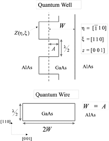
Specifically, we consider GaAs QWs of average width 16 ML, grown between wide AlAs barriers such that one of interfaces has steps along h direction. The interface geometry is illustrated in Fig. 1(a). Fig. 1(b) refers to the limiting case A = W, i. e., increasing the amplitude from 0 up to W, the system undergoes a transition from a QW structure with flat interfaces to a rectangular quantum wire of dimensions 2W and  . In order to get p.b.c. in this geometry, the system is modeled by orthorhombic cells of dimensions Nh, Nx and Nz (x = [1 1 0]). The interface shape function is given by

where A is the amplitude and Nh defines the wavelength of interface oscillations. Taking Nz = 60 ML guarantees convergence of our results to the infinite-width barriers situation, while Nx = 10 ML gives an adequate
  -points sampling to obtain the relevant states. The largest value considered for Nh is 14 ML, which corresponds to cells with 16,800 atoms. In reference [9] we found that the only relevant parameter controlling the QW optical behavior is the interface roughness r defined by

and Lh and Lx are the dimensions of the interface projection in the hx plane.
AlAs/GaAs/AlAs [0 0 1] QW profile of average width W, which one of the interfaces is flat and the other has a shape given by the function Z(h,x) with amplitude A and wavelength l (a). When A = W, the system becomes a quantum wire (b).
Results for the oscillator strength normalized to the flat interface value,  , as a function of the amplitude A for different wavelengths are shown in Fig. 2. We note that, for the step function (2), the roughness defined by (3) and (4), is r = A. In general, increasing A causes a decrease in f which eventually undergoes a transition to zero, as we can see in the Fig. 2 for l = 8 (triangles) and 12 ML (squares). When l is sufficiently large, ³ 14 ML (pentagons correspond to this value), we observe the usual decrease in f with A, up to a critical value AC » 8 ML, when f starts increasing with A. We interpret this effect by investigating the wavefunction behavior as a function of the interface roughness. The real-space wavefunctions in the tight-binding approach
are defined by their expansion coefficients Ca in the atomic-like orbitals a (a = s, px, py, pz, s*) at the zinc-blende atomic sites = (h, x, z). It is convenient to define the group-III sublattice sites as (hIII, xIII, z), and the group-V sites as (hV, xV, z ±
 . The overall probability density distribution across the well may be described through the envelope function [10]:

Note that the sublattice dependence of the charge distribution is eliminated in (6)-(8).
Calculated variation of the oscillator strength of AlAs/GaAs/AlAs QW's of average width W = 16 ML as a function of the interface amplitude A. The interface profile is defined by a periodic step function. The oscillator strength is normalized to the flat interface values. Different symbols correspond to the considered function oscillation wavelength: l = 8
Our results for the |yEF(z)|2 corresponding to the |e1ñ state in a W=16 ML QW (vertical dashed lines) are given by Fig. 3. The interface widths for amplitudes A ¹ 0 are represented by the vertical dotted lines. We consider amplitudes in regions corresponding to both of the identified regimes: When f decreases with A ( f  regime) and when f increases (f
  regime). We note that AC » 8 ML is the critical amplitude where f begins to increase.
Wavefunction squared (in arbitrary units) of the first electron state in an AlAs/GaAs/AlAs QW of average width W = 16 ML (vertical dashed lines), for planar interfaces (a) and for the other structures such that one of the interfaces is planar and the other has a shape given by a periodic step function with amplitudes A = 4 ML (b), A = 8 ML (c), A = 12 ML (d) and A = 16 ML (e).
Fig. 3(a) corresponds to a QW with planar interfaces and consequently yEF(z) is symmetric with respect to the well center. Figures 3(b) and 3(c) show results in the f regime for one of the interfaces given by Z(h, x) with A = 4 and 8 ML (vertical dotted lines). We note that the asymmetry of the heterostructures pushes the electronic density away from the rough interfaces. As we see, the wavefunctions are more localized in A < z < W, i. e., outside the interface region.
For A = 8 ML (amplitude near to the minimum f in Fig. 2, about 57 % of |yEF(z)|2 is in A < z < W while 39 % is in 0 < z < A. Above AC, in the f regime, the situation is inverted. For A = 10 ML and we note a migration of the electronic density into the rough interface region. In Fig. 3(d) for A = 10 ML, 53% of |yEF(z)|2 are within 0 < z < A . Fig. 3(e) corresponds to the limiting case of a quantum wire in which A = W = 16 ML. In this case, |yEF(z)|2 is entirely inside the quantum wire and, because of the symmetry of the system, the wavefunction is symmetric with respect z. Therefore it is possible to identify the two regimes in the behavior of f with a predominantly quantum well (f ) or quantum wire (f ) character of the charge distribution in the GaAs region.
III Hydrostatic pressure effect on the optical properties of QWs with interface roughness
An optical behavior similar to the f regime was observed in hydrostatic pressure studies of luminescence from (311)A Al0.35Ga0.65As/GaAs QWs [7]. An enhancement of the PL intensity was obtained with increasing pressure P for (311)A QWs. Since these QWs have a rough interface pattern, we analyze heterostructures similar to those considered in this work under hydrostatic pressure to investigate if increasing P produces the observed enhancement in the optical efficiency of the QWs.
In order to compare our calculations to the luminescence experiment results we calculate, instead of f, the spontaneous emission intensity for the optical transition between |e1ñ and |h1ñ states in the QW,

where C is a constant and DE is the gap energy between |e1ñ and |h1ñ. We note that there is a correlation between I and the oscillator strength: I = C¢(DE)3f.
Applying hydrostatic pressure on a material induces a decrease in the interatomic distances. This implies a higher interaction between the atoms and consequently, the level energy positions are modified due to an increase in the off-diagonal Hamiltonian matrix elements. As suggested in Ref.[11], we incorporate the hydrostatic pressure assuming that the nearest neighbors Hamiltonian matrix elements, h, increase according to a power-law when the interatomic distances are reduced under pressure. If d0 and d are, respectively, the distances between the neighbors atoms at zero pressure and pressure P, then
As a first approximation, we can take the bulk modulus B as a linear function of the pressure, B = B0 + B0¢P. This leads to the Murnaghan's state equation:

Equations (10) and (11) give the energy dependence with pressure through the Hamiltonian matrix elements. A fitting of the experimental results for the energy gap variation in the G point with applied pressure in GaAs, ( ), at P = 0, yields the exponent a = 3.454 [11]. This value of a also leads to a dependence on hydrostatic pressure of GaAs X and L points energy and of the AlAs G, X and L points energy is in agreement with experiments.
In the experiments [7], the QW barriers were taken as AlxGa1-x with x = 0.35 and the applied pressure ranged from 0 to 10 kbar. The QW integrated luminescence intensity increased by about a factor of three in this pressure range, while the increase in the emission from the GaAs buffer layer was about 50%.
In our model, the bulk GaAs optical emission intensity calculated from (9) presents an almost linear increase, resulting in a 20% enhancement as P goes from 0 to 10 kbar, which is in qualitative agreement with experiment. We consider [0 0 1]-grown QWs with W = 16 ML and alloy barriers with x = 0.30, which are comparable to the experimentally studies QWs geometry, but grown along a different direction. The calculated emission intensity for flat or rough-interfaces QWs shows essentially the same behavior as obtained for bulk GaAs, namely a 20% increase in the studied pressure range.
IV Conclusions
By analyzing our results shown in Figures 2 and 3, we conclude that the oscillator strength behavior with increasing A for large l is due to a quantum well to quantum wire crossover in the heterostructures. The first optical transition in the wire is dipole - allowed. Starting from a QW with flat interfaces (where f is maximum), the increase of A produces a decrease of f in the quantum well regime. The crossover into the quantum wire regime is identified by a cusp in f, followed by an increase in f with A.
For QWs under pressure, although we obtain an increase in the emission intensity with increasing pressure, our results give a much weaker effect than observed experimentally [7]. A possible explanation for this discrepancy is that we consider band-to-band transitions, and electron-hole interactions are not taken into account. The measured luminescence increase could be an excitonic effect, which of course is not considered here.
References
[1] W. Braun and K. H. Ploog, J. Appl. Phys. 75, 1993 (1994).
[2] W. Braun, A. Trampert, L. Daweritz and K. H. Ploog, Phys. Rev. B 55, 1689 (1997).
[3] A. Ourmazd and J. Cunningham, Phys. Rev. Lett. 65, 2318 (1990).
[4] B. Koiller, R. Osório and L. M. Falicov, Phys. Rev. B 43, 4170 (1991); B. Koiller e R. B. Capaz, Phys. Rev. Lett., 74, 769 (1995).
[5] P. Vogl, H. P. Hjalmarson and J. D. Dow, J. Phys. Chem. Solids 44, 365 (1983).
[6] B. Koiller, A. S. Martins and H. Chacham, Appl. Phys. Lett. 69 (1996).
[7] S. L. S. Freire, L. A. Cury, F. M. Matinaga and M. V. B. Moreira, accept to publication in Physica Status Solidi B Proceedings of the VII - High Pressure Semiconductor Physics Conference.
[8] K. Reirnann, Jap. J. App. Phys. 32, Suppl. 32-1, 64 (1993).
[9] T. G. Dargam and B. Koiller, Solid State Commun. 105, 211 (1998).
[10] T. G. Dargam, R. B. Capaz and B. Koiller, Phys. Review B 15, 9625 (1997).
[11] R. B. Capaz, J. P. von der Weid and B. Koiller, Appl. Phys. Lett. 60, 704, (1992).
- [1] W. Braun and K. H. Ploog, J. Appl. Phys. 75, 1993 (1994).
- [2] W. Braun, A. Trampert, L. Daweritz and K. H. Ploog, Phys. Rev. B 55, 1689 (1997).
- [3] A. Ourmazd and J. Cunningham, Phys. Rev. Lett. 65, 2318 (1990).
- [4] B. Koiller, R. Osório and L. M. Falicov, Phys. Rev. B 43, 4170 (1991);
- B. Koiller e R. B. Capaz, Phys. Rev. Lett., 74, 769 (1995).
- [5] P. Vogl, H. P. Hjalmarson and J. D. Dow, J. Phys. Chem. Solids 44, 365 (1983).
- [6] B. Koiller, A. S. Martins and H. Chacham, Appl. Phys. Lett. 69 (1996).
- [7] S. L. S. Freire, L. A. Cury, F. M. Matinaga and M. V. B. Moreira, accept to publication in Physica Status Solidi B Proceedings of the VII - High Pressure Semiconductor Physics Conference.
- [8] K. Reirnann, Jap. J. App. Phys. 32, Suppl. 32-1, 64 (1993).
- [9] T. G. Dargam and B. Koiller, Solid State Commun. 105, 211 (1998).
- [10] T. G. Dargam, R. B. Capaz and B. Koiller, Phys. Review B 15, 9625 (1997).
- [11] R. B. Capaz, J. P. von der Weid and B. Koiller, Appl. Phys. Lett. 60, 704, (1992).
Publication Dates
-
Publication in this collection
23 Feb 2001 -
Date of issue
Dec 1999
History
-
Received
06 Feb 1999