Abstracts
Silicon-based quantum-computer architectures have attracted attention because of their promise for scalability and their potential for synergetically utilizing the available resources associated with the existing Si technology infrastructure. Electronic and nuclear spins of shallow donors (e.g. phosphorus) in Si are ideal candidates for qubits in such proposals due to the relatively long spin coherence times. For these spin qubits, donor electron charge manipulation by external gates is a key ingredient for control and read-out of single-qubit operations, while shallow donor exchange gates are frequently invoked to perform two-qubit operations. More recently, charge qubits based on tunnel coupling in P+2 substitutional molecular ions in Si have also been proposed. We discuss the feasibility of the building blocks involved in shallow donor quantum computation in silicon, taking into account the peculiarities of silicon electronic structure, in particular the six degenerate states at the conduction band edge. We show that quantum interference among these states does not significantly affect operations involving a single donor, but leads to fast oscillations in electron exchange coupling and on tunnel-coupling strength when the donor pair relative position is changed on a lattice-parameter scale. These studies illustrate the considerable potential as well as the tremendous challenges posed by donor spin and charge as candidates for qubits in silicon.
semiconductors; quantum computation; nanoelectronic devices; spintronics; nanofabrication; donors in silicon
Arquiteturas de computadores quânticos baseadas em silício vêm atraindo atenção devido às suas perspectivas de escalabilidade e utilização dos recursos já instalados associados à tecnologia do Si. Spins eletrônicos e nucleares de doadores rasos (por exemplo fósforo) em Si são candidatos ideais para bits quânticos (qubits) nestas propostas, devido aos tempos de coerência relativamente longos dos spins em matrizes de Si. Para estes qubits de spin, a manipulação da carga do elétron do doador por eletrodos externos é um ingrediente importante para controle e leitura das operações de um-qubit, enquanto que as portas de troca são frequentemente invocadas para as operações de dois-qubits. Mais recentemente, qubits de carga baseados no tunelamento do elétron no íon molecular P+2 em Si foram também propostos. Discutimos aqui as operações elementares envolvidas na computação quântica baseada em doadores rasos em Si, levando em consideração as peculiaridades da estrutura eletrônica do Si, em particular a degenerescência sextupla do mínimo da banda de condução. Mostramos que a interferência quântica entre estes seis estados não afeta significativamente as operações envolvendo um único doador, mas leva a oscilações no acoplamento de troca e no acoplamento via tunelamento quando a posição relativa do par é modificada na escala de distâncias do parâmetro de rede. Nossos estudos ilustram as potencialidades bem como os enormes desafios envolvidos na implementação de qubits de spin e carga em Si.
semiconductores; computação quântica; dispositivos nano-eletrônicos; spintrônica; nanofabricação; doadores em silício
PHYSICAL SCIENCES
Silicon-based spin and charge quantum computation
Belita KoillerI,* * Member Academia Brasileira de Ciências ; Xuedong HuII; Rodrigo B. CapazI; Adriano S. MartinsIII; Sankar Das SarmaIV
IInstituto de Física, Universidade Federal do Rio de Janeiro, Cx. Postal 68.528, 21945-970 Rio de Janeiro, Brasil
IIDepartment of Physics, University at Buffalo, SUNY, Buffalo, NY, 14260-1500, USA
IIIInstituto de Física, Universidade Federal Fluminense, 24210-340 Niterói, RJ, Brasil
IVCondensed Matter Theory Center, Department of Physics, University of Maryland, College Park, MD 20742-4111, USA
Correspondence Correspondence to Belita Koiller E-mail: bk@if.ufrj.br
ABSTRACT
Silicon-based quantum-computer architectures have attracted attention because of their promise for scalability and their potential for synergetically utilizing the available resources associated with the existing Si technology infrastructure. Electronic and nuclear spins of shallow donors (e.g. phosphorus) in Si are ideal candidates for qubits in such proposals due to the relatively long spin coherence times. For these spin qubits, donor electron charge manipulation by external gates is a key ingredient for control and read-out of single-qubit operations, while shallow donor exchange gates are frequently invoked to perform two-qubit operations. More recently, charge qubits based on tunnel coupling in P+2 substitutional molecular ions in Si have also been proposed. We discuss the feasibility of the building blocks involved in shallow donor quantum computation in silicon, taking into account the peculiarities of silicon electronic structure, in particular the six degenerate states at the conduction band edge. We show that quantum interference among these states does not significantly affect operations involving a single donor, but leads to fast oscillations in electron exchange coupling and on tunnel-coupling strength when the donor pair relative position is changed on a lattice-parameter scale. These studies illustrate the considerable potential as well as the tremendous challenges posed by donor spin and charge as candidates for qubits in silicon.
Keywords: semiconductors, quantum computation, nanoelectronic devices, spintronics, nanofabrication, donors in silicon.
RESUMO
Arquiteturas de computadores quânticos baseadas em silício vêm atraindo atenção devido às suas perspectivas de escalabilidade e utilização dos recursos já instalados associados à tecnologia do Si. Spins eletrônicos e nucleares de doadores rasos (por exemplo fósforo) em Si são candidatos ideais para bits quânticos (qubits) nestas propostas, devido aos tempos de coerência relativamente longos dos spins em matrizes de Si. Para estes qubits de spin, a manipulação da carga do elétron do doador por eletrodos externos é um ingrediente importante para controle e leitura das operações de um-qubit, enquanto que as portas de troca são frequentemente invocadas para as operações de dois-qubits. Mais recentemente, qubits de carga baseados no tunelamento do elétron no íon molecular P+2 em Si foram também propostos. Discutimos aqui as operações elementares envolvidas na computação quântica baseada em doadores rasos em Si, levando em consideração as peculiaridades da estrutura eletrônica do Si, em particular a degenerescência sextupla do mínimo da banda de condução. Mostramos que a interferência quântica entre estes seis estados não afeta significativamente as operações envolvendo um único doador, mas leva a oscilações no acoplamento de troca e no acoplamento via tunelamento quando a posição relativa do par é modificada na escala de distâncias do parâmetro de rede. Nossos estudos ilustram as potencialidades bem como os enormes desafios envolvidos na implementação de qubits de spin e carga em Si.
Palavras-chave: semiconductores, computação quântica, dispositivos nano-eletrônicos, spintrônica, nanofabricação, doadores em silício.
1 INTRODUCTION
Most of the computer-based encryption algorithms presently in use to protect systems accessible to the public, in particular over the Internet, rely on the fact that factoring a large number into its prime factors is so computationally intensive that it is practically impossible. These systems would be vulnerable if faster factoring schemes became viable. The development by Shor, about a decade ago, of a quantum algorithm that can factorize large numbers exponentially faster than the available classical algorithms (Shor 1994) thus could make the public key encryption scheme potentially vulnerable, and has naturally generated widespread interest in the study of quantum computing and quantum information processing (Nielsen and Chuang 2000, DiVincenzo 1995, Ekert and Jozsa 1996, Steane 1998, Bennett and DiVincenzo 2000). The exponential speedup of Shor's algorithm is due to the intrinsic quantum parallelism in the superposition principle and the unitary evolution of quantum mechanics. It implies that a computer made up of entirely quantum mechanical parts, whose evolution is governed by quantum mechanics, would be able to carry out in reasonably short time prime factorization of large numbers that is prohibitively time-consuming in classical computation, thus revolutionizing cryptography and information theory. Since the invention of Shor's factoring algorithm, it has also been shown that error correction can be done to a quantum system (Shor 1995, Steane 1996), so that a practical quantum computer (QC) does not have to be forever perfect to be useful, as long as quantum error corrections can be carried out. These two key mathematical developments have led to the creation of the new interdisciplinary field of quantum computation and quantum information.
The elementary unit of a QC is the quantum bit, or qubit, which is a two-level quantum system (|0ñ and |1ñ). Contrary to a classical bit which is in one of the binary states, either 0 or 1, the state of a qubit could be any quantum-mechanical superposition state of this two-level system: a|0ñ + b|1ñ, where a and b are complex numbers constrained to the normalization |a|2 + |b|2 = 1 . The computation process in a QC consists of a sequence of operations, or logical gates, in terms of locally tailored Hamiltonians, changing the states of the qubits through quantum mechanical evolution. Quantum computation generally involves logical gates that may affect the state of a single qubit, i.e. changing {ain,bin} into {aout,bout}, as well as multiple-qubit gates. The formalism for quantum information processing is substantially simplified by the following result proven by Barenco et al (Barenco et al. 1995): A universal set of gates, consisting of all one-qubit quantum gates and a single two-qubit gate, e.g. the controlled-NOT (C-NOT) gate, may be combined to perform any logic operation on arbitrarily many qubits.
The physical realization of qubits begins with demonstration of one-qubit gates and the C-NOT quantum gate for one and two qubits. After successfully performing these basic logic operations at the one and two qubits stage, the next step is to scale up, eventually achieving a large scale QC of ~ 106 qubits. So far, 15 is the largest number for which Shor's factorization was implemented in a physical system (Vandersypen et al. 2001). This factorization required coherent control over seven qubits.
Many physical systems have been proposed as candidates for qubits in a QC, ranging from those in atomic physics, optics, to those in various branches of condensed matter physics (DiVincenzo 1995, Ekert and Jozsa 1996, Steane 1998, Bennett and DiVincenzo 2000). Among the more prominent solid state examples are electron or nuclear spins in semiconductors ( uti
uti et al. 2004, Das Sarma et al. 2001, Hu 2004, Das Sarma et al. 2005), including electron spin in semiconductor quantum dots (Loss and DiVincenzo 1998, Imamoglu et al. 1999) and donor electron or nuclear spins in semiconductors (Kane 1998, Vrijen et al. 2000).
Silicon donor-based QC schemes are particularly attractive because doped silicon makes a natural connection between present microelectronic devices and perspective quantum mechanical devices. Doping in semiconductors has had significant technological impact for the past fifty years and is the basis of current mostly silicon-based microelectronics technology. As transistors and integrated circuits decrease in size, the physical properties of the devices are becoming sensitive to the actual configuration of impurities (Voyles et al. 2002). In this context, the first proposal of donor-based silicon QC by Kane (Kane 1998), in which the nuclear spins of the monovalent 31P impurities in Si are the qubits, has naturally created considerable interest in revisiting all aspects of the donor impurity problem in silicon, particularly in the Si:31P system.
In principle, both spin and electronic orbital degrees of freedom can be used as qubits in semiconductor nanostructures. A great advantage of orbital (or equivalently, charge) qubits is that qubit-specific measurements are relatively simple because measuring single charge states involves well-developed experimental techniques using single-electron transistors (SET) or equivalent devices (Grabert and Devoret 1992). A major disadvantage of solid state charge qubits is that these orbital states are highly susceptible to interactions with the environment that contains all the stray or unintended charges inevitably present in the device, so that the decoherence time is generally far too short (typically picoseconds to nanoseconds) for quantum error correction to be useful. A related problem is that inter-qubit coupling, which is necessary for the implementation of two-qubit gate operations essential for quantum computation, is often the long-range dipolar coupling for charge qubits. This makes it difficult to scale up the architecture, since decoherence grows with the scaling-up as more and more qubits couple to each other via the long-range dipolar coupling. However, the strong interactions make the orbital states an excellent choice for studying qubit dynamics and qubit coupling in the solid state nanostructure environment.
Spin qubits in semiconductor nanostructures have complementary advantages (and disadvantages) compared with charge qubits based on quantized orbital states. A real disadvantage of spin qubits is that a single electron spin (not to mention a single nuclear spin) is difficult to measure rapidly, although there is no fundamental principle against the measurement of a Bohr magneton. The great advantage of spin qubits is the very long spin coherence times, which even for electron spins can be milliseconds in silicon at low temperatures. In addition to the coherence advantage, spin qubits also have a considerable advantage that the exchange gate (Loss and DiVincenzo 1998), which provides the inter-qubit coupling, is exponentially short-ranged and nearest-neighbor in nature, thus allowing precise control and manipulation of two-qubit gates. There is no fundamental problem arising from the scaling-up of the QC architecture since exchange interaction couples only two nearest-neighbor spin qubits independent of the number of qubits.
We provide here a brief perspective on spin and charge qubits in silicon with electron spins or charge states in shallow P donor levels in Si being used as qubits. In Sec. 2 we present some background on the classic problem of the shallow donor in silicon, describing it through two complementary approaches: The effective mass theory and the tight-binding formalism. In Sec. 3 we analyze the response of the donor electron to an applied uniform field, and conclude that electric field control over the donor electron does not present additional complications due to the Si host electronic structure characteristics. Sec. 4 is devoted to the exchange coupling for a donor pair in Si, which is highly sensitive to interdonor positioning. We review the basic formalism leading to this behavior, and also describe attempts to overcome it, namely by considering donors in strained Si, and by refining the theoretical formalism for the problem. The feasibility of charge qubits based on  molecular ions in Si is investigated in Sec. 5, where we focus on the tunnel coupling and charge coherence in terms of electron-phonon coupling.
2 SINGLE DONOR IN SILICON
Silicon is a group-IV element, so that when a Si atom at a lattice site R0 in the bulk is replaced by a group-V element like P, the simplest description for the electronic behavior of the additional electron is a hydrogenic model, in which this electron is subject to the Si crystal potential perturbed by a screened Coulomb potential produced by the impurity ion:

The static dielectric constant of Si,  = 12.1, indicates that the donor confining potential is weaker than the bare hydrogen atom potential, leading to larger effective Bohr radii and smaller binding energies, so that donors are easily ionized (also known as shallow donors).
In this section we briefly review basic properties concerning the donor ground state wavefunction within two complementary formalisms: The effective mass theory (EMT), which is a reciprocal space formalism, and the tight-binding (TB) formalism, which is a real space scheme. EMT exploits the duality between real and reciprocal space, where delocalization in real space leads to localization in k-space. Since shallow donor wavefunctions are expected to extend over several lattice constants in real space (the lattice parameter of Si crystal is aSi = 5.4 Å), it is written in terms of the bulk eigenstates for one or a few k-vectors at the lower edge of the conduction band. The TB description is a microscopic atomistic formalism, in which the basis set for the donor wavefunction expansion consists of atomic orbitals localized at the individual atoms.
2.I EFFECTIVE MASS THEORY
The bound donor electron Hamiltonian for an impurity at site R0 is written as

The first term,
SV, is the single-valley Kohn-Luttinger Hamiltonian (Kohn 1957), which includes the single particle kinetic energy, the Si periodic potential, and the screened impurity Coulomb potential in Eq. (1). The second term of Eq. (2), VO, includes the inter-valley coupling effects due to the presence of the impurity potential.
Following the EMT assumptions, the donor electron eigenfunctions are written on the basis of the six unperturbed Si band edge Bloch states fm = um(r) [the conduction band of bulk Si has six degenerate minima (µ = 1,...,6), located along the GX axes of the Brillouin zone at |km| ~ 0.85(2p/aSi) from the G point]:

In Eq. (3), Fm(r R0) are envelope functions centered at R0, for which we adopt the anisotropic Kohn-Luttinger form, e.g., for µ = z, Fz(r) = exp{[(x2 + y2)/a2 + z2/b2]1/2}/ . The effective Bohr radii a and b are variational parameters chosen to minimize ESV =
  , leading to a = 25 Å, b = 14 Å, in agreement with the expected increased values with respect to bare atoms.
The
SV ground state is six-fold degenerate. This degeneracy is lifted by the valley-orbit interactions included here inVO, leading to the nondegenerate (A1-symmetry) ground state in (3). Fig. 1 gives the charge density  for this state, where the periodic part of the conduction band edge Bloch functions were obtained from ab-initio calculations, as described by Koiller et al. 2004. The impurity site R0, corresponding to the higher charge density, is at the center of the frame. It is interesting that, except for this central site, regions of high charge concentration and atomic sites do not necessarily coincide, because the charge distribution periodicity imposed by the plane-wave part of the Bloch functions is 2p/kµ, incommensurate with the lattice period.
2.2 TIGHT-BINDING DESCRIPTION FOR P DONOR IN SILICON
The TB Hamiltonian for the impurity problem is written as:

where i and j label the atomic sites, µ and n denote the atomic orbitals and spins, and  , cin are creation and annihilation operators for the atomic states. We do not include spin-orbit corrections, thus all terms are spin-independent. The matrix elements
  define the on-site energies and first and second neighbors hopping for the bulk material, for which we take the parametrization given by Klimeck et al. 2000. The donor impurity potential is included in the perturbation term U(Ri), the same as Eq. (1), but in a discretized form restricted to the lattice sites:

where ri is the distance of site i to the impurity site. At the impurity site (ri = 0), the perturbation potential is assigned the value U0, a parameter describing central cell effects characteristic of the substitutional species. We take U0 = 1.48 eV, which leads to the experimentally observed binding energy of P in Si, 45.6 meV (Martins et al. 2004). Detailed comparison of the TB donor ground state wavefunction with Kohn-Luttinger EMT, performed by Martins et al. 2004, shows that the EMT oscillatory behavior coming from the interference among the plane-wave part of the six fm is well captured by the TB envelope function. The good agreement between TB and K&L is limited to distances from the impurity site larger than a few lattice parameters ( ~ 1 nm). Closer to the impurity, particularly at the impurity site, the TB results become considerably larger than the K&L prediction, in agreement with experiment.
The TB problem is numerically solved by restricting the real-space description to a supercell in which periodic boundary conditions are applied. For the single donor problem, the supercell is taken to be large enough so that convergence in the results is achieved (Martins et al. 2004, 2002).
3 ELECTRIC-FIELD CONTROL OF SHALLOW DONOR IN SILICON
Logic operations in quantum computer architectures based on P donors in Si involve the response of the bound electron wavefunctions to voltages applied to a combination of metal gates separated by a barrier material (e.g. SiO2) from the Si host. The A-gate (according to the nomenclature originally proposed by Kane 1998), placed above each donor site, pulls the electron wavefunction away from the donor, aiming at partial reduction (Kane 1998) or total cancellation (Skinner et al. 2003) of the electron-nuclear hyperfine coupling in architectures where the qubits are the 31P nuclear spins. In a related proposal based on the donor electron spins as qubits (Vrijen et al. 2000), the gates drive the electron wavefunction into regions of different g-factors, allowing the exchange coupling between neighboring electrons to be tuned.
We present here a simplified model of the A-gate operation by considering the Si:P system under a uniform electric field and near a barrier. Following Martins et al. 2004, we describe the electronic problem within the TB approach, where the basic Hamiltonian is given in Eq. (4), with the perturbation term including the Coulomb potential as in Eq. (5), plus the contribution of a constant electric field of amplitude E applied along the [00 ] direction:
The overall preturbation potential along the z-axis is represented in Fig. 2. We take the origin of the potential at the impurity site, R0, at the center of the supercell. Periodic boundary conditions lead to a discontinuity in the potential at the supercell boundary zi = ZB, where ZB is half of the supercell length along [001] or, equivalently, the distance from the impurity to the Si/barrier interface. The potential discontinuity, VB = 2|e|EZB, actually has a physical meaning in the present study: It models the potential due to the barrier material layer above the Si host (see Fig. 2).
A description of the A-gate operations may be inferred from the behavior of the TB envelope function squared (this function is defined at each lattice site as the sum of the squared TB wavefunction expansion coefficients at this site) at the impurity site under applied field E, normalized to the zero-field value:

The notation here indicates that this ratio should follow a behavior similar to that for the hyperfine coupling constants between the donor nucleus and electron with (A) and without (A0) external field. The ratio in (7) is plotted in Fig. 3(a) for three values of the impurity depth with respect to the Si/barrier interface. Calculations for ZB=10.86 nm were performed with cubic supercells (L = 40 aSi), while for ZB= 5.43 and 21.72 nm tetragonal supercells with Lx = Ly = 40 aSi and Lz = 20 aSi and 80 aSi respectively were used. At small field values we obtain a quadratic decay of A/A0 with E, in agreement with the perturbation theory results for the hydrogen atom. At large enough fields,  becomes vanishingly small, and the transition between the two regimes is qualitatively different according to ZB: For the largest values of ZB we get an abrupt transition at a critical field Ec, while smaller ZB (e.g. ZB = 5.43 nm) lead to a smooth decay, similar to the one depicted by Kane (Kane 1998). In this latter case, we define Ec as the field for which the curve A/A0 vs E has an inflection point, where A/A0 ~ 0.5, thus Ec(5.43 nm) = 1030 kV/cm. We find that the decrease of Ec with ZB follows a simple rule Ec µ 1/ZB, as given by the solid line in Fig. 3(b).

The above results may be understood within a simple picture of the electron in a double well potential, the first well being most attractive at the impurity site, V(R0 = 0) = U0, and the second well at the barrier interface, V(z = ZB) = VB/2 = |e|EZB neglecting the Coulomb potential contribution at the interface. An internal barrier separates the two wells and, for a fixed E, this internal barrier height and width increase with ZB. Deep donor positioning leads to a weaker coupling between the states localized at each well, even close to level degeneracy, resulting the level crossing behavior of the two lowest donor-electron states illustrated in Fig. 4(a). For a donor positioned closer to the interface, the internal barrier gets weaker, enhancing the coupling between levels localized in each well and leading to wavefunction superposition and to the anticrossing behavior illustrated in Fig. 4(b). The scaling of Ec with 1/ZB may also be understood assuming that the critical field corresponds to the crossing of the ground state energies of two wells: The Coulomb potential well and an approximately triangular well at the barrier. Since the relative depths of the wells increases with EZB, and assuming that the ground states energies are fixed with respect to each well's depth, the Ec µ 1/ZB behavior naturally results.

The minimum gap at the anticrossing in Fig. 4(b) is ~ 9.8 meV, which allows for adiabatic control of the electron by the A-gate within switching times of the order of picoseconds, as discussed by Martins et al. 2004.. This is a perfectly acceptable time for the operation of A-gates in spin-based Si QC, given the relatively long electron spin coherence times (of the order of a few ms) in Si.
We remark that the Bloch phases interference behavior in the donor wavefunctions are well captured in the TB wavefunctions, and that the results above demonstrate that electric field control over single donor wavefunctions, such as proposed in A-gate operations, (Kane 1998, Vrijen et al. 2000, Skinner et al. 2003) do not present additional complications due to the Si band structure. The only critical parameter is the donor positioning below the Si/barrier interface, which should be chosen and controlled according to physical criteria such as those discussed here.
4 DONOR ELECTRON EXCHANGE IN SILICON
An important issue in the study of donor-based Si QC architecture is coherent manipulations of spin states as required for the quantum gate operations. In particular, two-qubit operations, which are required for a universal QC, involve precise control over electron-electron exchange (Loss and DiVincenzo 1998, Kane 1998, Vrijen et al. 2000, Hu and Das Sarma 2000). Such control can presumably be achieved by fabrication of donor arrays with well-controlled positioning and surface gate potential (O'Brien et al. 2001, Schofield et al. 2003, Buehler et al. 2002, Schenkel et al. 2003). However, electron exchange in bulk silicon has spatial oscillations (Andres et al. 1981, Koiller et al. 2002) on the atomic scale due to valley interference arising from the particular six-fold degeneracy of the bulk Si conduction band. These exchange oscillations place heavy burdens on device fabrication and coherent control (Koiller et al. 2002a), because of the very high accuracy and tolerance requirements for placing each donor inside the Si unit cell, and/or for controlling the external gate voltages.
The potentially severe consequences of the exchange-oscillation problem for exchange-based Si QC architecture motivated us and other researchers to perform theoretical studies with increasingly sophisticated formalisms, incorporating perturbation effects due to applied strain (Koiller et al. 2002b) or gate fields (Wellard et al. 2003). These studies, all performed within the standard Heitler-London (HL) formalism (Slater 1963), essentially reconfirm the originally reported difficulties (Koiller et al. 2002a) regarding the sensitivity of the electron exchange coupling to precise atomic-level donor positioning, indicating that they may not be completely overcome by applying strain or electric fields. The sensitivity of the calculated exchange coupling to donor relative position originates from interference between the plane-wave parts of the six degenerate Bloch states associated with the Si conduction-band minima. More recently (Koiller et al. 2004) we have assessed the robustness of the HL approximation for the two-electron donor-pair states by relaxing the phase pinning at donor sites.
In this section, we first review the main results regarding exchange coupling for a donor pair in relaxed bulk Si, and its high sensitivity to interdonor positioning. We then discuss ways to overcome this behavior, namely considering donors in strained Si and the more general floating-phase HL formalism. We show that strain may partially alleviate the exchange oscillatory behavior, but it cannot entirely overcome the problem. From the floating-phase HL approach results, our main conclusion is that, for all practical purposes, the previously adopted HL wavefunctions are robust, and the exchange sensitivity to donor positioning obtained by Koiller et al. 2002a, b and Wellard et al. 2003 persists in the more sophisticated theory by Koiller et al. 2004.
4.I DONOR ELECTRON EXCHANGE IN RELAXED BULK SILICON
The HL approximation is a reliable scheme to calculate electron exchange for a well-separated pair of donors (interdonor distance much larger than the donor Bohr radii) (Slater 1963). Within HL, the lowest energy singlet and triplet wavefunctions for two electrons bound to a donor pair at sites RA and RB, are written as properly symmetrized and normalized combinations of  and
and  [as defined in Eq.(3)]
where S is the overlap integral and the upper (lower) sign corresponds to the singlet (triplet) state. The energy expectation values for these states,  , give the exchange splitting through their difference, J = Et Es. We have previously derived the expression for the donor electron exchange splitting (Koiller et al. 2004, 2002b), which we reproduce here:

where R = RA RB is the interdonor position vector and  µn (R) are kernels determined by the envelopes and are slowly varying functions of R (Koiller et al. 2002a, b). Note that Eq. (9) does not involve any oscillatory contribution from um(r), the periodic part of the Bloch functions (Koiller et al. 2004, Wellard et al. 2003). The physical reason for that is clear from (3): While the plane-wave phases of the Bloch functions are pinned to the donor sites, leading to the cosine factors in (9), the periodic functions um are pinned to the lattice, regardless of the donor location.
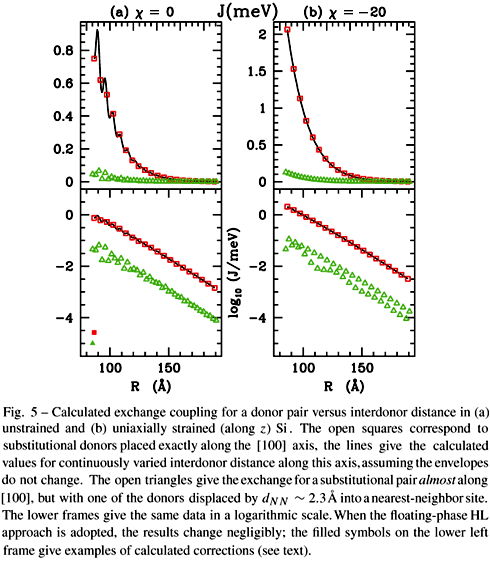
As an example of the consequences of the sensitivity of exchange to interdonor relative positioning, we present in Fig. 5(a) a case of practical concern involving unintentional donor displacements into nearest-neighbor sites, when the two donors belong to different fcc sublattices. The open squares in Fig. 5(a) give J(R) for substitutional donors along the [100] axis, while the open triangles illustrate the different-sublattice positioning situation, namely R = R0 +  NN with R0 along the [100] axis and NN ranging over the four nearest-neighbors of each R0 (dNN = |NN| = aSi
  /4 ~ 2.34 Å). The lower panel of the figure presents the same data on a logarithmic scale, showing that nearest-neighbor displacements lead to an exchange coupling reduction by one order of magnitude when compared to J(R0).
4.2 STRAINED SILICON
The extreme sensitivity of J(R) to interdonor positioning can be eliminated for on-lattice substitutional impurities in uniaxially strained Si (e.g. along the z axis) commensurately grown over Si-Ge alloys if inter-donor separation R remains parallel to the interface x-y plane (Koiller et al. 2002b). The strain is accommodated in the Si layer by increasing the bond-length components parallel to the interface and decreasing those along z, breaking the cubic symmetry of the lattice and lowering the six-fold degeneracy of the conduction band minimum to two-fold. In this case, the valley populations in the donor electron ground state wave function in Eq. (3) are not all equal to 1/ , but are determined from a scalar valley strain parameter c, which quantifies the amount of strain. Fig. 5(b) gives J(R) in uniaxially strained (along z direction) Si for c = 20 (corresponding to Si grown over a Si-Ge alloy with 20% Ge-content) for the same relative positioning of the donor pairs as in Fig. 5(a). Notice that the exchange coupling is enhanced by about a factor of 2 with respect to the relaxed Si host, but the order-of-magnitude reduction in J caused by displacements of amplitude dNN into nearest-neighbor sites still persists as NN is not parallel to the x-y plane.
4.3 FLOATING-PHASE HEITLER-LONDON APPROACH
In previous studies by Koiller et al. 2002a, b, as in the standard HL formalism presented in subsection 4.1, it is implicitly assumed that the phases  in Eq. (3) remain pinned to the respective donor sites R0 = RA and RB, as we adopt single donor wavefunctions to build the two-electron wavefunction. Although phase pinning to the donor substitutional site is required for the ground state of an isolated donor (A1 symmetry) in order to minimize single electron energy, this is not the case for the lower-symmetry problem of the donor pair. In order to minimize the energy of the two-donor system, here we allow the phases to shift by an amount dR along the direction of the interdonor vector R = RB RA, so that the single-particle wavefunctions in Eq. (8) become

and

We take dR as a variational parameter to minimize Es and Et. Since the phases in Eq.(3) are responsible for the sensitivity of the exchange coupling to donor positioning in Si, this more general variational treatment might lead to changes in the previously reported (Koiller et al. 2002a, b, Wellard et al. 2003) behavior of the two-donor exchange splitting J = Et Es.
Minimization of the total energy for the particular geometry where the donor pair is 87 Å apart along the [100] direction leads the singlet energy decrease of 270 neV, and the triplet energy decrease of 6 neV. This results in an increase in J by 264 neV, given by the solid square in the lower left hand side frame of Fig. 5. The floating phases variational scheme leads to a reduction in both singlet and triplet states energy, therefore the net variation in J is positive (negative) if the triplet energy reduction is smaller (larger) than the singlet. The solid triangle in Fig. 5 corresponds to a case of negative variation, obtained when one of the donors in the above geometry is displaced into a nearest-neighbor site. Note that the corrections are more than three orders of magnitude smaller than the calculated J within standard HL. In other words, for all practical purposes the fixed-phase standard HL approximation is entirely adequate for the range of interdonor distances of interest for QC applications.
From the perspective of current QC fabrication efforts, ~ 1 nm accuracy in single P atom positioning has been recently demonstrated (Schofield et al. 2003), representing a major step towards the goal of obtaining a regular donor array embedded in single crystal Si. Exchange coupling distributions consistent with such accuracy are presented by Koiller and Hu 2004, indicating that even such small deviations ( ~ 1 nm) in the relative position of donor pairs can still lead to significant changes in the exchange coupling, favoring J ~ 0 values. Severe limitations in controlling J would come from "hops" into different substitutional lattice sites. Therefore, precisely controlling of exchange gates in Si remains an open (and severe) challenge. As suggested by Koiller et al. 2003, spatially resolved micro-Raman spetroscopy might provide a valuable diagnostic tool to characterize local values of exchange coupling between individual spin qubits.
5 CHARGE QUBITS IN SILICON
Successful coherent manipulation of electron orbital states in GaAs has been achieved for electrons bound to donor impurities (Cole et al. 2000) as well as electrons in double quantum dots (Hayashi et al. 2003). There were also suggestions of directly using electron orbital states in Si as the building blocks for quantum information processing (Hollenberg et al. 2004a, b). Specifically, a pair of phosphorus donors that sit relatively close to each other (so as to have sizable wave function overlap) form an effective hydrogen molecule in Si host material. Charge qubits may be defined by ionizing one of the bound electrons, thus leading to a double well potential filled with a single electron: The single electron ground state manifold, whether it is the two states localized in each of the wells or their symmetric and anti-symmetric combinations, can then be used as the two-level system forming a charge qubit (Ekert and Jozsa 1995, Tanamoto 2001). The advantage of such a charge qubit is that it is easy to manipulate and detect, while its disadvantage, as already mentioned above, is the generally fast charge decoherence as compared to spin.
In this section we discuss the feasibility of the charge qubit in Si, focusing on single qubit properties in terms of the tunnel coupling between the two phosphorus donors, and charge decoherence of this system in terms of electron-phonon coupling. We take into consideration the multi-valley structure of the Si conduction band and explore whether valley interference could lead to potential problems or advantages with the operations of charge qubits, such as difficulties in the control of tunnel coupling similar to the control of exchange in two-electron systems discussed in Sec. 4, or favorable decoherence properties through vanishing electron-phonon coupling.
5.I THE MOLECULE IN SILICON
We study the simple situation where a single electron is shared by a donor pair, constituting a molecule in Si. The charge qubit here consists of the two lowest energy orbital states of an ionized P2 molecule in Si with only one valence electron in the outermost shell shared by the two P atoms. The key issue to be examined is the tunnel coupling and the resulting coherent superposition of one-electron states, rather than the entanglement among electrons, as occurs for an exchange-coupled pair of electrons.
The donors are at substitutional sites RA and RB in an otherwise perfect Si structure. In the absence of an external bias, we write the eigenstates for the two lowest-energy states as a superposition of single-donor ground state wavefunctions [as given in Eq. (3)] localized at each donor, yA (r) and yB (r), similar to the standard approximation for the  molecular ion (Slater 1963). The symmetry of the molecule leads to two eigenstates on this basis, namely the symmetric and antisymmetric superpositions
As described by Hu et al. 2004, the energy gap between these two states may be written as

where S is the overlap integral between yA (r) and yB (r). For R = RA RB  a,b, the amplitudes dm(R) are monotonically decaying functions of the interdonor distance R, and S
  1. The dependence of dm on |R| is qualitatively similar to the symmetric-antisymmetric gap in the
  molecule, namely an exponential decay with power-law prefactors. The main difference here comes from the cosine factors, which are related to the oscillatory behavior of the donor wavefunction in Si arising from the Si conduction band valley degeneracy, and to the presence of two pinning centers.
Fig. 6 shows the calculated gaps as a function of R for a donor pair along two high-symmetry crystal directions.
Two points are worth emphasizing here, which are manifestly different from the corresponding hydrogenic molecular ion behavior: (i) DSAS is an anisotropic and fast oscillatory function of R; (ii) the sign of DSAS may be positive or negative depending on the precise value of R. The characteristics mentioned in point (i) are similar to the exchange coupling behavior previously discussed for the two-electrons neutral donor pair (Koiller et al. 2004, 2002a, b). Point (ii) implies that the  molecular ion ground state in Si may be symmetric (as in the molecular ion case) or antisymmetric depending on the separation between the two P atoms. Note that for the two-electron case, the ground state is always a singlet (i.e. a symmetric two-particle spatial part of the wavefunction with the spin part being antisymmetric), implying that the exchange J is always positive for a two-electron molecule. For a one-electron ionized molecule, however, the ground state spatial wavefunction can be either symmetric or antisymmetric.
Fig. 7 shows the normalized probability distribution for the DSAS gap values when the first donor is kept fixed at RA and the second donor is placed at a site 20 lattice parameters away (~ 108.6 Å), along the [100] axis. This target configuration is indicated by an arrow in Fig. 6. We allow the second donor position RB to visit all possible substitutional diamond lattice positions within a sphere of radius Ru centered at the attempted position. Our motivation here is to simulate the realistic fabrication of a molecular ion with fixed inter-atomic distance in Si with the state of the art Si technology, in which there will always be a small (Ru ~ 1 3 nm) uncertainty in the precise positioning of the substitutional donor atom within the Si unit cell. We would like to estimate the resultant randomness or uncertainty in DSAS arising from this uncertainty in RB. For Ru = 0, i.e., for R = 20 aSi , DSAS ~ 2.4 meV, given by the arrow in Fig. 7. We incorporate the effect of small uncertainties by taking Ru = 1nm, corresponding to the best reported degree of accuracy in single P atom positioning in Si (Schofield et al. 2003). These small deviations completely change the qubit gap distribution, as given by the histogram in Fig. 7, strongly peaked around zero. Further increasing Ru leads to broader distributions of the gap values, though still peaked at zero (Hu et al. 2004). We conclude that the valley interference between the six Bloch states leads to a strong suppression of the qubit fidelity since the most probable DSAS tends to be zero.
A very small DSAS is undesirable in defining the two states |0ñ and |1ñ forming the charge qubit. If we take them to be the symmetric and anti-symmetric states given in Eq. (12), the fact that they are essentially degenerate means that, when one attempts to initialize the qubit state at |0ñ, a different combination a|0ñ + b|1ñ might result. Well defined qubits may still be defined under a suitable applied external bias, so that the electron ground state wavefunction is localized around one of the donors, say at lattice site RA, and the first excited state is localized around RB.
Single qubit rotations, used to implement universal quantum gates (Nielsen and Chuang 2000), might in principle be achieved by adiabatic tunneling of the electron among the two sites under controlled axially aligned electric fields through bias sweeps (Barrett and Milburn 2003). When, at zero bias, the ground state is not well separated by a gap from the first excited state, severe limitations are expected in the adiabatic manipulation of the electron by applied external fields. In other words, the fidelity of the single qubit system defining the quantum two-level dynamics will be severely compromised by the valley interference effect.
5.2 ELECTRON-PHONON COUPLING
Two key decoherence channels for charge qubits in solids are background charge fluctuations and electron-phonon coupling (Hayashi et al.2003). The former is closely related to the sample quality (e.g., existences of stray charges and charged defects in the system) and is extrinsic, while the latter is intrinsic. Here we focus on the electron-phonon coupling. A critical question for the molecular ion in Si is whether the Si bandstructure and the associated charge density oscillations (Koiller et al. 2004) lead to any significant modification of the electron-phonon coupling matrix elements. The relevant terms for the electron-phonon interaction in Si takes the form:

where D is the deformation constant, rm is the mass density of the host material, V is the volume of the sample, aq and  are phonon annihilation and creation operators, and r(q) is the Fourier transform of the electron density operator. For the two-donor situation, where we are only interested in the two lowest energy single-electron eigenstates, the electron-phonon coupling Hamiltonian is conveniently written in this quasi-two-level basis in terms of the Pauli spin matrices sx and sz (where spin up and down states refer to the two electronic eigenstates, labeled {|+ñ,|ñ}):

Here the term proportional to sx can lead to transition between the two electronic eigenstates and is related to relaxation; while the term proportional to sz only causes energy renormalization of the two electronic levels, but no state mixing, so that it only leads to pure dephasing for the electronic charge states.
Calculations of the matrix elements involved in Eq. (15), reported by Hu et al. 2004, lead to the conclusion that the electron-phonon coupling for a molecular ion in Si formally behaves very similarly to that for a single electron trapped in a GaAs double quantum dot. For example, the relaxation matrix element is proportional to
where the more complicated multi-valley bandstructure of Si and the strong inter-valley coupling introduced by the phosphorus donor atoms only strongly affect the off-site (thus small) contribution to the electron-phonon coupling, so that they do not cause significant changes in the overall electron-phonon coupling matrix elements. Therefore, available estimates (Barrett and Milburn 2003, Fedichkin and Fedorov 2004) of decoherence induced by electron-phonon coupling based on a single-valley hydrogenic approximation in the system in Si should be valid. In other words, the multi-valley quantum interference effect does not provide any particular advantage (or disadvantage) for single qubit decoherence in the Si:P donor charge-based QC architecture.
6 SUMMARY
In summary, we have briefly reviewed physical aspects related to some of the relevant building blocks for the implementation of donor spin and charge qubits in silicon: Electric field control of a single donor, the exchange gate for two spin qubit operations, control and coherence of charge qubits. Our results indicate that, although some of the operations may be implemented as originally conceived, the spin and charge qubits based on donors in silicon pose immense challenges in terms of precise nanostructure fabrications because of the degenerate nature of the silicon conduction band. Further studies of fabrication and innovative alternative approaches are imperative in order to fully realize the potential of donor-based QC architectures.
ACKNOWLEDGMENTS
This work was supported by Conselho Nacional de Desenvolvimento Científico e Tecnológico (CNPq), Instituto do Milênio de Nanociências and Fundação Carlos Chagas Filho de Amparo à Pesquisa do Estado do Rio de Janeiro (FAPERJ) in Brazil, Advanced Research and Development Activity (ARDA) and Laboratory for Physical Sciences National Security Agency (LPS-NSA) at the University of Maryland, and by The Army Research Office Advanced Research and Development Activity (ARO-ARDA) at the University at Buffalo and the University of Maryland.
Manuscript received on February 10, 2005; accepted for publication on March 7, 2005; contributed by BELITA KOILLER*
- ANDRES K, BHATT RN, GOALWIN P, RICE TM AND WALSTEDT RE. 1981. Low-temperature magnetic-susceptibility of Si-P in the non-metallic region. Phys Rev B 24: 244-260.
- BARENCO A, BENNETT CH, CLEVE R, DIVINCENZO DP, MARGOLUS N, SHOR P, SLEATOR T, SMOLIN JA AND WEINFURTER H. 1995. Elementary gates for quantum computation. Phys Rev A 52: 3457-3467.
- BARRETT SD AND MILBURN GJ. 2003. Measuring the decoherence rate in a semiconductor charge qubit. Phys Rev B 68: 155307.
- BENNETT CH AND DIVINCENZO DP. 2000. Quantum information and computation. Nature 404: 247-255.
- BUEHLER TM, MCKINNON RP, LUMPKIN NE, BRENNER R, REILLY DJ, MACKS LD, HAMILTON AR, DZURAK AS AND CLARK RG. 2002. A self-aligned fabrication process for silicon quantum computer devices. Nanotechnology 13: 686-690.
- COLE BE, WILLIAMS JB, KING BT, SHERWIN MS AND STANLEY CR. 2000. Coherent manipulation of semiconductor quantum bits with terahertz radiation. Nature 410: 60-63.
- DAS SARMA S, FABIAN J AND ZUTIC I. 2001. Spin electronics and spin computation. Solid State Commun 119: 207-215.
- DAS SARMA S, DE SOUSA R, HU X AND KOILLER B. 2005. Spin quantum computation in silicon nanostructures. Solid State Commun 113: 737-746.
- DIVINCENZO DP. 1995. Quantum Computation. Science 270: 255.
- EKERT AK AND JOZSA R. 1996. Quantum computation and Shor's factoring algorithm. Rev Mod Phys 68: 733-753.
- FEDICHKIN L AND FEDOROV A. 2004. Error rate of a charge qubit coupled to an acoustic phonon reservoir. Phys Rev A 69: 032311.
- GRABERT H AND DEVORET MH. 1992. Single Charge Tunneling, Plenum, New York.
- HAYASHI T, FUJUSAWA T, CHEONG HD, JEONG YH AND HIRAYAMA Y. 2003. Coherent Manipulation of Electronic States in a Double Quantum Dot. Phys Rev Lett 91: 226804.
- HOLLENBERG LCL, DZURAK AS, WELLARD CJ, HAMILTON AR, REILLY DJ, MILBURN GJ AND CLARK RG. 2004a. Charge-based quantum computing using single donors in semiconductors. Phys Rev B 69: 113301.
- HOLLENBERG LCL, WELLARD CJ, PAKES CI AND FOWLER AG. 2004b. Single-spin readout for buried dopant semiconductor qubits. Phys Rev B 69: 233301.
- HU X. 2004. Quantum Dot Quantum Computing, arXiv:cond-mat/0411012. Springer Lecture Notes Series (in press).
- HU X AND DAS SARMA S. 2000. Hilbert-space structure of a solid-state quantum computer: Two-electron states of a double-quantum-dot artificial molecule. Phys Rev A 61: 062301.
- HU X AND DAS SARMA S. 2003. Overview of spin-based quantum dot quantum computation. Phys Stat Sol (b) 238: 360-365.
- HU X, KOILLER B AND DAS SARMA S. 2004. Charge qubits in semiconductor quantum computer architectures: Tunnel coupling and decoherence, arXiv:cond-mat/0412340.
- IMAMOGLU A, AWSCHALOM DD, BURKARD G, DIVINCENZO DP, LOSS D, SHERWIN M AND SMALL A. 1999. Quantum information processing using quantum dot spins and cavity QED. Phys Rev Lett 83: 4204-4207.
- KANE BE. 1998. A silicon-based nuclear spin quantum computer. Nature 393: 133-137.
- KLIMECK G, BOWEN RC, BOYKIN TB, LAZARO CS, CWIK TA AND STOICA A. 2000. Si tight-binding parameters from genetic algorithm fitting. Superlattices Microstruct 27: 77-88.
- KOHN W. 1957. Shallow impurity states in silicon and germanium, in Solid State Physics, vol. 5, SEITZ F AND TURNBULL D ed. New York: Academic Press, p. 257-320.
- KOILLER B AND HU X. 2004. Nanofabrication aspects of silicon-based spin quantum gates. IEEE Transactions in Nanotechnology 4: 113-115.
- KOILLER B, HU X AND DAS SARMA S. 2002a. Exchange in silicon-based quantum computer architecture. Phys Rev Lett 88: 027903.
- KOILLER B, HU X AND DAS SARMA S. 2002b. Strain effects on silicon donor exchange: Quantum computer architecture considerations. Phys Rev B 66: 115201.
- KOILLER B, HU X, DREW HD AND DAS SARMA S. 2003. Disentangling the Exchange Coupling of Entangled Donors in the Silicon Quantum Computer Architecture. Phys Rev Lett 90: 067401.
- KOILLER B, CAPAZ RB, HU X AND DAS SARMA S. 2004. Shallow donor wavefunctions and donor-pair exchange in silicon: Ab initio theory and floating-phase Heitler-London approach. Phys Rev B 70: 115207.
- LOSS D AND DIVINCENZO DP. 1998. Quantum computation with quantum dots. Phys Rev A 57: 120-126.
- MARTINS AS, MENCHERO JG, CAPAZ RB AND KOILLER B. 2002. Atomistic description of shallow levels in semiconductors. Phys Rev B 65: 245205.
- MARTINS AS, CAPAZ RB AND KOILLER B. 2004. Electric field control and adiabatic evolution of shallow-donor impurities in silicon. Phys Rev B 69: 085320.
- NIELSEN MA AND CHUANG IL. 2000. Quantum computation and quantum information (Cambridge Univ. Press, Cambridge, UK).
- O'BRIEN JL, SCHOFIELD SR, SIMMONS MY, CLARK RG, DZURAK AS, CURSON NJ, KANE BE, MCALPINE NS, HAWLEY ME AND BROWN GW. 2001. Towards the fabrication of phosphorus qubits for a silicon quantum computer. Phys Rev B 64: 161401.
- PRIVMAN V, VAGNER ID AND KVENTSEL G. 1998. Quantum computation in quantum-Hall systems. Phys Lett A 239: 141-146.
- SCHENKEL T, PERSAUD A, PARK SJ, NILSSON J, BOKOR J, LIDDLE JA, KELLER R, SCHNEIDER DH, CHENG DW AND HUMPHRIES DE. 2003. Solid state quantum computer development in silicon with single ion implantation. Journal of Applied Physics 94: 7017-7024.
- SCHOFIELD SR, CURSON NJ, SIMMONS MY, RUEß FJ, HALLAM T, OBERBECK L AND CLARK RG. 2003. Atomically precise placement of single dopants in Si. Phys Rev Lett 91: 136104.
- SHOR PW. 1994. Polynomial-time algorithms for prime factorization and discrete logarithms on a quantum computer, in: S. GOLDWASSER ed., Proceedings of the 35th Annual Symposium on the Foundations of Computer Science (IEEE Computer Society, Los Alamitos), p. 124-134.
- SHOR PW. 1995. Scheme for reducing decoherence in quantum computer memory. Phys Rev A 52: R2493-R2496.
- SKINNER AJ, DAVENPORT ME AND KANE BE. 2003. Hydrogenic spin quantum computing in silicon: A digital approach. Phys Rev Lett 90: 087901.
- SLATER JC. 1963. Quantum Theory of Molecules and Solids, vol. 1, McGraw-Hill, New York.
- STEANE A. 1998. Quantum computing. Rep Prog Phys 61: 117-173.
- STEANE AM. 1996. Error correcting codes in quantum theory. Phys Rev Lett 77: 793-797.
- TANAMOTO T. 2000. Quantum gates by coupled asymmetric quantum dots and controlled-NOT-gate operation. Phys Rev A 61: 022305.
- TANAMOTO T. 2001. One- and two-dimensional N-qubit systems in capacitively coupled quantum dots. Phys Rev A 64: 062306.
- VANDERSYPEN LMK, STEFFEN M, BREYTA G, YANNONI CS, SHERWOOD MH AND CHUANG IL. 2001. Experimental realization of Shor's quantum factoring algorithm using nuclear magnetic resonance. Nature 414: 883-887.
- VOYLES PM, MULLER DA, GRAZUI JL, CITRIN PH AND GROSSMANN H-JL. 2002. Atomic-scale imaging of individual dopant atoms and clusters in highly n-type bulk Si. Nature 416: 826-829.
- VRIJEN R, YABLONOVITCH E, WANG K, JIANG HW, BALANDIN A, ROYCHOWDHURY V, TAL MOR AND DIVINCENZO DP. 2000. Electron-spin-resonance transistors for quantum computing in silicon-germanium heterostructures. Phys Rev A 62: 012306.
- WELLARD CJ, HOLLENBERG LCL, PARISOLI F, KETTLE L, GOAN H-S, MCINTOSH JAL AND JAMIESON DN. 2003. Electron exchange coupling for single-donor solid-state spin qubits. Phys Rev B 68: 195209.
- ZUTIC I, FABIAN J AND DAS SARMA S. 2004. Spintronics: Fundamentals and applications. Rev Mod Phys 76: 323-410.
Publication Dates
-
Publication in this collection
09 May 2005 -
Date of issue
June 2005
History
-
Accepted
07 Mar 2005 -
Received
10 Feb 2005