Abstracts
The semiconducting properties of passive films formed on AISI 304 stainless steel and Alloy 600 in borate buffer solution were studied by capacitance (Mott-Schottky approach) and photocurrent measurements. Oxide films formed on 304 stainless steel in air at 350 ºC have also been studied. The results obtained show that, in all cases the electronic structure of the films is comparable to that of a p-n heterojunction in which the space charges developed at the metal-film and film-electrolyte interfaces have also to be considered. This is in accordance with analytical results showing that the oxide films are in all cases composed of an inner region rich in chromium oxide and an outer region rich in iron oxide.
stainless steel; alloy 600; oxide films; capacitance measurements; photocurrent; heterojunction
Estudaram-se as propriedades semicondutoras de filmes passivos formados em aço inoxidável AISI 304 e em ligas de base Ni (Alloy 600) em soluções tampão de borato. Os filmes foram estudados por medidas de capacidade (Mott-Schottky ) e de fotocorrente. Estudaram-se também filmes formados em aço inoxidável AISI 304 por oxidação ao ar, à temperatura de 350ºC. Os resultados mostram que a estrutura electrónica dos filmes é comparável à de uma heterojunção do tipo p-n, onde as cargas de espaço desenvolvidas nas interfaces filme -- metal e filme -- electrólito devem ser consideradas. O estudo electroquímico está de acordo com os resultados analíticos que demonstram que os filmes de óxido são, em todos os casos, compostos por uma região interna rica em óxido de crómio e por uma região externa rica em óxido de ferro.
Article
Semiconducting Properties of Oxide and Passive Films Formed on AISI 304 Stainless Steel and Alloy 600
M. G. S. Ferreira * * e-mail: mgferreira@cv.ua.pt ,a,b, M. Da Cunha Beloa, N. E. Hakikia, G. Goodleta, M. F. Montemora and A. M. P. Simõesa * e-mail: mgferreira@cv.ua.pt
a Department of Chemical Engineering, Instituto Superior Técnico, 1049-001 Lisboa, Portugal
b Department of Ceramics and Glass Engineering, University of Aveiro, 3810-193 Aveiro, Portugal
Estudaram-se as propriedades semicondutoras de filmes passivos formados em aço inoxidável AISI 304 e em ligas de base Ni (Alloy 600) em soluções tampão de borato. Os filmes foram estudados por medidas de capacidade (Mott-Schottky ) e de fotocorrente. Estudaram-se também filmes formados em aço inoxidável AISI 304 por oxidação ao ar, à temperatura de 350ºC. Os resultados mostram que a estrutura electrónica dos filmes é comparável à de uma heterojunção do tipo p-n, onde as cargas de espaço desenvolvidas nas interfaces filme ¾ metal e filme ¾ electrólito devem ser consideradas. O estudo electroquímico está de acordo com os resultados analíticos que demonstram que os filmes de óxido são, em todos os casos, compostos por uma região interna rica em óxido de crómio e por uma região externa rica em óxido de ferro.
The semiconducting properties of passive films formed on AISI 304 stainless steel and Alloy 600 in borate buffer solution were studied by capacitance (Mott-Schottky approach) and photocurrent measurements. Oxide films formed on 304 stainless steel in air at 350 ºC have also been studied. The results obtained show that, in all cases the electronic structure of the films is comparable to that of a p-n heterojunction in which the space charges developed at the metal-film and film-electrolyte interfaces have also to be considered. This is in accordance with analytical results showing that the oxide films are in all cases composed of an inner region rich in chromium oxide and an outer region rich in iron oxide.
Keywords: stainless steel, alloy 600, oxide films, capacitance measurements, photocurrent, heterojunction
Introduction
The passive films formed on stainless steels and Ni-based alloys reveal a semiconductive behaviour1-6 and therefore, the electronic properties should play an important role in the corrosion resistance. Under certain conditions, the electronic structure of these films can be more accurately described as a bi-layer composed of a n-type outer region containing iron oxide and hydroxide and a p-type inner region containing chromium oxide.6,7 Nickel oxide is also present in both alloys mainly in the external layers of the film, although a much larger Ni/Fe ratio is found in the case of the Alloy 600.
In this work capacitence and a comparison is made between the electronic structure of films formed on 304 stainless steel at 350 ºC and that of passive films formed in borate buffer solution. Electrochemical and photoelectrochemical results obtained for very thin passive films on 304 stainless steel and Alloy 600 are presented as well as those obtained in the case of oxide films formed on 304 stainless steel in air at temperature of 350 ºC.
Experimental
AISI 304 stainless steel and Alloy 600 passive films were formed in borate buffer solution at 0.8 V and 0.3 V (respectively) vs. SCE for 2 h and thermally grown oxide films were formed in air at controlled temperature of 350 ºC inside a furnace, for 2 h at atmospheric pressure. The chemical composition of the 304 stainless steel and Alloy 600 used is shown in Table 1. The working electrodes were plate shaped (1 cm2) and were mounted in an acrylic resin. The surface was abraded with wet SiC paper of decreasing grit size (400, 600, 1200) and was finally polished with alumina (2mm), rinsed in distilled water, ultrasonically cleaned and dried in air. A classical cell with three electrodes was utilized, in which the platinum wire counter-electrode had an area of 1 cm2 and the reference electrode was a saturated calomel electrode (SCE).
The analytical experiments were made using a 310 F Microlab (VG Scientific), equipped with a field emission type electron gun and a concentric hemispherical analyser. Auger spectra were taken using a 10 keV, 50 nA primary electron beam. Ion etching was performed at a pressure of 1x10⁻⁷ mBar using high purity argon. The etching current was approximately 0.75 mA/mm2. The etched area was a crater with a diameter of 1 mm, whereas the electron beam had a spatial resolution of » 100 nm. The electron beam was aligned with the centre of the sputtered region. Although the roughness of the surface increases with the sputtered depth, the very high spatial resolution of the electron beam limits the deleterious effects of long sputtering. In the case of passive films atomic densities were determined by a quantitative approach based on the sequential sputtering model by Sanz and Hoffmann.8
AFM images of the film formed on stainless steel at 350 ºC were obtained using a Topometrix 2010 "Discoverer" equipment working in non-contact mode with a silicon nitride tip.
The capacitance measurements were performed at 1580 Hz in the potential range 0.5 V to ¾1.5 V (vs. SCE). Polarisation was applied by successive steps of 50 mV in the cathodic direction. A potentiostat (EG&G 273) and a double phase synchronous detector (Brookdeal 5208 lock-in amplifier) with an internal oscillator working in a large frequency range (5Hz-100 kHz) were used. The principle is to apply simultaneously a perturbing signal DU (10 mV rms) to the cell via the potentiostat and to the reference chain. The response is compared to DU dephased by Df and Df+p/2.
Photoelectrochemical measurements were performed by using a 150 W xenon lamp and a 1200/mm grating monochromator (Jobin Yvon H25). The photocurrents were generated by focusing the light with a fused silica lens through a quartz window of the electrochemical cell, onto the working electrode. The lock-in technique, allowed the separation of the photocurrent from the passive current by chopping the light at a constant frequency (19Hz) and feeding the signal as well as the current output of the potentiostat to the lock-in amplifier. The photocurrent spectra were obtained on specimens polarized at 0 V vs. SCE by scanning the wavelength of the light in steps of 10 nm from 350 nm to 750 nm.
The capacitance measurements and the photoelectrochemical study were carried out at room temperature (22 ºC) under continuous de-aeration with high-purity nitrogen in a buffer solution of composition H3BO3 (0.05mol L-1) + Na2B4O7.10H2 O(0.075 mol L-1) and pH 9.2. This solution was used in the formation and study of the thin passive films (in-situ experiments) and in the study of the thermally grown oxide films.
In the interpretation of the capacitance results we introduce the Mott-Sckottky approach, which assumed that the capacitance response is controlled by the band bending and can be described by the variation of the space charge capacitance under depletion conditions. In the case of a semiconducting passive film/electrolyte interface, the Mott-Schottky relationship has to take into account the contribution of the Helmholtz layer capacitance CH according to9

where Nq represents the donor or acceptor density, e the dielectric constant of the passive film, e0 the vacuum permittivity, e the elementary charge for electrons (- e for holes), k the Boltzmann constant, T the absolute temperature and UFB the flatband potential.
In the study by photoelectrochemistry we consider that in the case of passive films the contribution to the photocurrent of the hole-electron pair formed in the bulk region is negligible, the quantum efficiency h, defined as the ratio between the photocurrent Iph and the incident photon flux F0 of energy hn, is given by the following relation 10,11

where A is a constant, e the elementary charge, w the thickness of the space charge layer and Eg the bandgap energy. The exponent n depends on the type of the transition between the valence band and the conduction band. The analysis of the photocurrent spectra obtained with the passive films shows that n=2 is the most appropriate value to represent a photoelectrochemical behaviour according to equation 2. This value of n corresponds to indirect transitions in crystallized solids and also to non-direct transitions in amorphous materials.
Results
AISI 304 stainless steel
Auger analysis and AFM characterisation. Figure 1 depicts the Auger depth profiles obtained on a film formed on 304 stainless steel at 350 °C. The film is composed of an external Fe oxide rich region and an inner Cr oxide rich region. The film thickness is about 25 nm. The value of the maximum atomic concentration for Cr is about 20%. This means that a Cr-Fe mixed oxide is always present in the inner region of the film.
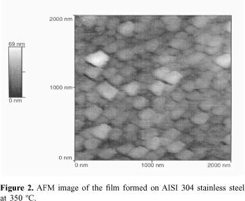
Figure 2 shows an AFM image of the same film. It can be seen that the film morphology shows round shaped nodules.
Figure 3 depicts the Auger depth profiles for passive films formed on 304 stainless steel in borate buffer solution, obtained by applying the sequential layer-sputtering model. The passive film has a duplex character with an inner region rich in chromium oxide and an outer region rich in iron oxide. The concentration of the chromium and iron are very similar to the concentrations of these elements in pure Cr2O3 and Fe2O3 respectively. It also appears that the inner layer of the passive film is composed of practically pure chromium oxide. The reasons for the chromium enrichment in the inner layer are due to a higher mobility of iron ions in the film as well as a higher stability of iron oxide in the electrolyte used as compared to chromium oxide.
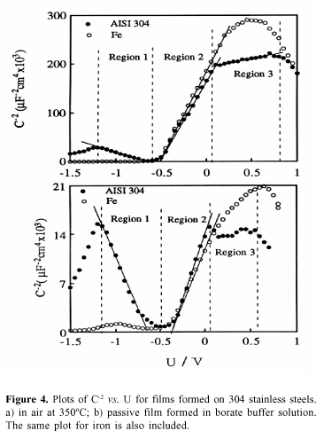
Capacitance measurements. Figure 4a shows the C-2vs. U plot obtained for the oxide film formed on 304 stainless steel, at 350 °C. The capacitance measurements reveal the existence of a straight line with a positive slope for potentials higher than -0.5 V and with a negative slope for potentials lower than -0.5 V. This means that the oxide films behave as n-type semiconductor in the more noble potential region and as a p-type semiconductor in the lower potential region.
Another feature of the Mott-Schottky plot depicted in Figure 4a is the existence of a break at » 0 V. This break of the plot was explained assuming the existence of two kinds of donors one very close to the conduction band and the other below the conduction band.12
From the slope of the straight line of the C-2vs. U plot, the donor and acceptor densities of the Fe and Cr oxide layers can be calculated. Using e = 12 for the dielectric constant of chromium oxide and iron oxide, the values of ND and NA are respectively 0.5x10²⁰ and 2.3x1020 cm-3.
Figure 4b shows that the plot of C-2vs. U for a passive film formed on 304 stainless steel reveals a similar capacitance behaviour to that of an oxide film thermally grown at 350 °C. In both cases the negative and positive slopes of the Mott-Schottky plots show that the film behaves as a p-type semiconductor at potentials lower than ¾0.5 V and as an n-type semiconductor at potentials higher than ¾0.5 V. Note that from the slope of the straight lines of the C-2vs. U plots, the donor and acceptor densities obtained for the passive film (formed at 0.8V) are 2.5 x 10²⁰ and 2.3 x 1020 cm-3. The value of ND is higher than that obtained for the film grown at 350 ºC, revealing that the number of defects is larger in the case of the passive film.
In both cases in Figure 4 the plot of C-2vs. U relative to the iron oxide is depicted, showing that iron oxide only reveals n-type semiconductivity.
The use of pure metals and Fe-Cr alloys helps in the understanding of the capacitance behaviour of the passive film formed on 304 stainless steel. Figure 5 shows that the flat band potential of the chromium passive film is situated at about 0.5 V. This potential is close to the electrochemical potential of transpassivation of stainless steels. On the other hand the flat band potential of the passive iron film is situated at about ¾0.5 V (Figure 4). When the passive film is formed on stainless steel the capacitance response at potentials higher than ¾0.5 V is controlled by the outer iron oxide layer of the film. Conversely, at potentials lower than ¾0.5 V the capacitance response reflects the semiconducting properties of the inner chromium oxide layer. In fact the flat band potential determined by the intercept of the negative slope in the Mott-Schottky plot is an apparent flat band potential for chromium oxide. This means that the metallic substrate-passive film interface is always in depletion (a Schottky barrier) at potentials lower than 0.5 V. At potentials higher than this potential, i.e. in the transpassive potential region of stainless steels, the same interface is in accumulation (an ohmic contact). This model is referred to in more detail in next section.
Photoelectrochemical measurements Figure 6 shows the spectra obtained when (hhn)1/2 is plotted against hn for the film formed at 350 ºC and for the passive film on 304 SS. The results show that the quantum efficiency increases with temperature. This agrees with the fact that the number of donors present in the external layers of the films decreases when the temperature is raised and can be associated to an enlargement of the space charge layer in the oxide films. By extrapolation of (hhn)1/2 to hn= 0, a threshold energy value around 2.3 eV is obtained in both cases. Thus, the absorption edge position does not depend on the formation temperature of the film.
Another feature of the spectra presented in Figure 6 is that the photoresponse evolution near the absorption edge is not a sharp one, and shows subgap absorption. This phenomenon is the well-known band tail, traditionally associated with crystalline defects, impurities, deep levels or localized states in the bandgap, when significant photocurrents are observed with sub bandgap illumination. Figure 6 shows the existence of a peak of photocurrent situated at 1.9 eV, e.g. for photon energies lower than Eg (in the sub-bandgap region). This peak can be associated to transitions from the valence band to the second donor level localized in the bandgap. In fact, taking into account that the energy bandgap value is 2.3 eV, it can be easily established13 that this level is situated at 0.4 eV below the conduction band. This interpretation supports the analysis of C-2vs. U plots in Figure 4. In fact, in the electrochemical potential scale, the position of this second donor level (0.4 V) corresponds approximately to the potential of 0 V.
Alloy 600
Auger analysis. According to published data7,14 the critical chromium concentration necessary to develop a protective Cr-oxide barrier at the film-metal interface is approximately the same (about 15%) for both Fe-Cr and Ni-Cr alloys. However, the films formed on Ni-based alloys are thinner than those formed on stainless steel.
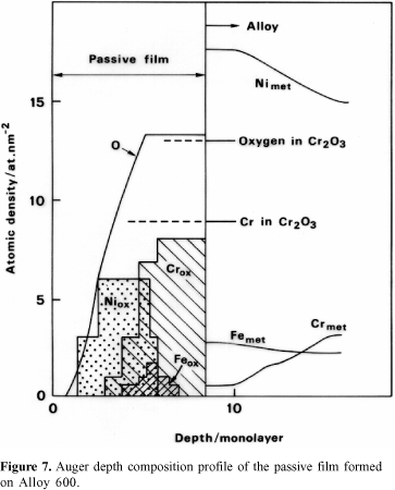
Figure 7 shows that the very thin film formed on Alloy 600 consists mainly of an inner layer of Cr2O3 developed in contact with the substrate and an external layer of Ni oxide. The latter is certainly covered by hydroxides. Iron oxide is detected in the intermediate part of the film, i.e., between the Cr-oxide layer and the Ni-oxide layer. Analytical results reveal Cr depletion underneath the passive film. This was also observed for stainless steel.15
Capacitance measurements.Figure 8 shows the results of the capacitance measurements on the passive films formed on Alloy 600, plotted as C-2vs. U, which are overlapped to the corresponding plot for AISI 304 SS. Two linear regions revealing Mott-Schottky behaviour are apparent in both cases and this can be related to the development of depletion layers promoted by band bending. When the films are polarized at more positive potentials they behave as a n-type semiconductor (positive slope) and when the polarization is in domain of the more negative potentials their behaviour is that of a p-type semiconductor (negative slope). The capacitance behaviour of the two alloys (SS and Alloy 600) is in this aspect very similar, although the capacitance values are lower for the Alloy 600.
Figure 9 shows that in the case of Alloy 600 the value of the capacitance at the flatband potential region is practically the same of the films formed on pure Ni. This seems to indicate that the film formed on the Alloy 600 depicts in this potential region a capacitance response essentially controlled by the Ni oxide contrarily to the film formed on SS. In the latter case the capacitance value at the flatband potential is 30 mF cm-2, which is representative of Helmholtz capacitance, CH. Therefore the contribution of the passive film to the measured capacitance is very weak (the film behaves as a conductor). Thus, although, Ni oxide is traditionally envisaged as a p-type semiconductor, its influence in the passive film in the range of potential showed can be compared to that of a dielectric. Under these considerations, the total measured capacitance can be considered as the equivalent capacitance of three serial capacitors:

where CNi is the capacitance corresponding to the Ni oxide.
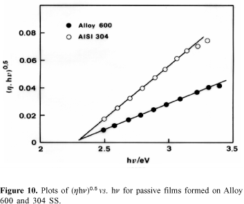
Photoelectrochemical measurements. Plots of spectral data according to equation 2 and presented in Figure10 show that the photoresponse of the passive film formed on 304 SS is higher than that of the passive film formed on Alloy 600. However, the bandgap energy is 2.3 eV for both materials.
Discussion
Thermally Grown Oxide Film
To explain the capacitance and photoelectrochemical results obtained account has to be taken of the concepts of band bending that are well established in semiconductor physics and semiconductor electrochemistry. Figure 11a gives a schematic representation of the band structure model for the thermally grown oxide film on 304 stainless steel. It can be assumed that the capacitance and photoelectrochemical responses reflect the influence of the space charge regions developed at the film-electrolyte and film-metal interfaces (interfaces I and III) and also at the heterojunction in the bulk of the film (interface II). The band model presented in Figure 11b explains how under the influence of the anodic polarization (at U>-0.5V), the slope of the C-2vs. U plots is modified (Figure 4). In fact the contribution of the second donor level in both thermally grown oxide films and very thin passive films is qualitatively similar. This means that the structural organisation, i.e. the lattice cell of the spinel is similar. Chromium is an alloying element that promotes the development of a chromium oxide of p-type semiconductivity in the inner part of the film in series with the n-type iron oxide layer developed in the outer part of the film. The two oxides in fact form a p-n heterojunction because they have different band gaps. However, the exact band structure model, which takes into account both the electronic transfer and the ionic transport of charges might be very complicated.
Passive Films
As can be observed for passive films the donor and acceptor doping densities are practically identical (» 2.5 x 1020 cm-3). It is important to remark that the passive film is formed under the influence of the applied potential U. Thus, because the Fermi potential remains constant through all parts of the film the electric potential y and the chemical potential m need to change in order to verify the basic relationships.

This is in contrast to the thermally grown films, where during film growth the Fermi level is not controlled by an applied potential.
For non-zero space charge the surface charge at the two interfaces of a passive film formed by a single oxide layer must be equal and opposite to the total space charge for overall charge conservation. On the other hand, according to experimental results, potential barriers (Schottky barriers) can be developed at both metal-film and film-electrolyte interfaces and also at the p-n heterojunction situated in the bulk of the film. If we assume that the film is stable, the height of the potential barrier at the metal-film and film-electrolyte interface is a function of the applied potential. That of the p-n heterojunction depends essentially on the structural defects and does not change under the influence of a polarization because the Fermi energy is constant across the heterojunction. In fact the structural defects at all the interfaces depend on the formation potential and also of the applied potential.
The electronic band structure model proposed in previous work7,16 considers that the flat band potentials of the inner (Cr oxide) and outer (Fe oxide) layers of the passive films are characterized by the same flat band potential situated at about ¾0.5 V. It was assumed that under an applied potential the passive film acts as a Schottky barrier above and below this flat band potential. Consequently the inner film-metal interface is in an accumulation condition at potentials higher than ¾0.5 V. This may be not true if we consider that the more accurate flat band potential of the metal-chromium oxide interface is situated at about 0.5 V, i.e. the lower potential of the transpassive region.
The schematic band structure models in Figure 12 allow us to compare the electronic structure created in the latter case for potentials lower and higher than ¾0.5 V. In Figure 12a the film-electrolyte interface is in a situation of accumulation at potentials lower than ¾0.5V. In Figure 12b the same interface is in a situation of depletion at potentials higher than -0.5V. The presence of localized states in the bandgap as well as surface states were not considered in the general model of Figure 12.
Conclusions
The electronic structure of the passive films formed on AISI 304 stainless steel and Alloy 600 as well as of those thermally grown on the former alloy is comparable to that of a p-n heterojunction in which space charges are developed. It is the presence of Cr oxide (p-type semiconductivity) and Fe oxide (n-type semiconductivity), respectively, in the internal and external layers of the films, that establishes the heterojunction.
Space charges are also developed at the metal-film and film-electrolyte interfaces; these are in equilibrium with the space charges created at the heterojunction in the case of passive films.
The proposed electronic structure models describe the two types of films studied. Both reveal similar structural organization, with similar lattice cells.
References
Received: March 9, 2002
Published on the web: August 1, 2002
- 1. Paola, A. Di; Electrochim. Acta 1989, 34, 203.
- 2. Simões, A.M.P.; Ferreira, M.G.S.; Rondot, B.; Cunha Belo, M. Da; J. Electrochem. Soc. 1990, 137, 82.
- 3. Sunseri, C.; Piazza, S.; Paola, A. Di; Quarto, F. Di; J. Electrochem. Soc. 1987, 134, 2410.
- 4. Paola, A. Di; Sunseri, C.; Quarto, F. Di; Corros. Sci. 1986, 26, 935.
- 5. Schumuki, P.; Bohni, H.; J. Electrochem. Soc 1992, 139, 1908.
- 6. Cunha Belo, M. Da; Hakiki, N.E.; Ferreira, M.G.S.; Electrochim. Acta 1999, 44, 2473.
- 7. Hakiki, N.E.; Boudin, S.; Rondot, B.; Cunha Belo, M. Da; Corros. Sci. 1995, 37, 1809.
- 8. Sanz, J.M.; Hofmann, S.; Surf. Interface Anal. 1986 ,8, 147.
- 9. Gryse, R. De; Gomes, W.P.; Cardon, F.; Vennik, J.; J. Electrochem. Soc. 1975, 122, 711.
- 10. Gartner, W.W.; Phys. Rev. 1959, 116, 84.
- 11. Butler, M.A.; J. Appl. Phys. 1977, 48, 1914.
- 12. Kennedy, J.H.; Frese, K.W.; J. Electrochem. Soc. 1987, 125, 723.
- 13. Hakiki, N.E.; Cunha Belo, M. Da; J. Electrochem. Soc. 1996, 143, 3088.
- 14. Boudin, S.; Vignes, J.L.; Lorang, G.; Cunha Belo, M. Da; Dlondiaux, G.; Mikhailov, S.M.; Jacobs, J.P.; Brongersma, H.H.; Surf. Interface Anal. 1994, 22, 462.
- 15. Lorang, G.; Cunha Belo, M. Da; Simões, A.M.P.; Ferreira, M.G.S.; J. Electrochem. Soc. 1994, 141, 3347.
- 16. Hakiki, N.E.; Rondot, B.; Cunha Belo, M. Da; C.R. Acad. Sci. Paris 1993, 317, Serie II, 457.
Publication Dates
-
Publication in this collection
06 Sept 2002 -
Date of issue
Aug 2002
History
-
Accepted
01 Aug 2002 -
Received
09 Mar 2002