Abstract
This work reports a study of the room-temperature synthesis of a SnO2/ZnO bilayer by magnetron sputtering. Morphological, optical, and electrical properties of the bilayer were investigated for different thicknesses of SnO2. Morphology was studied using profilometry and field emission scanning electron microscopy. The optical transmittances of the ZnO films and of the SnO2/ZnO combination were high (about 80%) in the visible, and the SnO2 film did not alter the optical properties of the ZnO, which would act as a transparent contact electrode in a perovskite solar cell.
Keywords:
ETL; Doped tin oxide; Solar energy; PSC
1. Introduction
Over the last few years, perovskite solar cells (PSCs) have attracted the attention of researchers in science and technology owing to their excellent energy conversion efficiencies11 Sahli F, Werner J, Kamino BA, Bräuninger M, Monnard R, Paviet-Salomon B, et al. Fully textured monolithic perovskite/silicon tandem solar cells with 25.2% power conversion efficiency. Nat Mater. 2018;17(9):820-6.
2 Chen Y, Meng Q, Zhang L, Han C, Gao H, Zhang Y, et al. SnO2-based electron transporting layer materials for perovskite solar cells: a review of recent progres. J Energy Chem. 2019;35:144-67.-33 Yang Y, Wu J, Guo P, Liu X, Guo Q, Liu Q, et al. Low-temperature sintered SnO2 electron transport layer for efficient planar perovskite solar cells. J Mater Sci Mater Electron. 2018;29(15):13138-47.. Despite this, several studies have indicated that the efficiency of PSCs depends on factors beyond the active layer, such as the optimization of the electron transport layer (ETL)22 Chen Y, Meng Q, Zhang L, Han C, Gao H, Zhang Y, et al. SnO2-based electron transporting layer materials for perovskite solar cells: a review of recent progres. J Energy Chem. 2019;35:144-67.. An ETL acts as a selective charge carrier layer, reducing the rate of recombination between electrons and holes. Different techniques may be used to synthesize ETLs, including the hydrothermic method33 Yang Y, Wu J, Guo P, Liu X, Guo Q, Liu Q, et al. Low-temperature sintered SnO2 electron transport layer for efficient planar perovskite solar cells. J Mater Sci Mater Electron. 2018;29(15):13138-47.,44 Xu Y, Liu T, Li Z, Feng B, Li S, Duan J, et al. Preparation and photovoltaic properties of perovskite solar cell based on ZnO nanorod arrays. Appl Surf Sci. 2016;388(3):89-96., thermal vaporization55 Ke W, Zhao D, Grice CR, Cimaroli AJ, Ge J, Tao H, et al. Efficient planar perovskite solar cells using room-temperature vacuum-processed C60 electron selective layers. J Mater Chem A Mater Energy Sustain. 2015;3(35):17971-6., electrodeposition66 Chen JY, Chueh CC, Zhu Z, Chen WC, Jen AKY. Low-temperature electrodeposited crystalline SnO2 as an efficient electron-transporting layer for conventional perovskite solar cells. Sol Energy Mater Sol Cells. 2017;164:47-55., atomic layer deposition77 Kavan L, Steier L, Gratzel M. Ultrathin buffer layers of SnO2 by atomic layer deposition: perfect blocking function and thermal stability. J Phys Chem C. 2017;121(1):342-50. http://dx.doi.org/10.1021/acs.jpcc.6b09965.
http://dx.doi.org/10.1021/acs.jpcc.6b099...
, pulsed laser deposition88 Chen Z, Yang G, Zheng X, Lei H, Chen C, Ma J, et al. Bulk heterojunction perovskite solar cells based on room temperature deposited hole-blocking layer: suppressed hysteresis and flexible photovoltaic application. J Power Sources. 2017;351:123-9. and magnetron sputtering (MS)99 Sung YM. Deposition of TiO2 blocking layers of photovoltaic cell using rf magnetron sputtering technology. Energy Procedia. 2013;34:582-8.. Among these methods, MS provides compact, cheap ETLs and shows potential for industrial-scale production. Moreover, some properties, such as photoelectric performance of the solar cells, transmittance in the visible region, surface roughness, and I-V characteristics (current density as a function of potential difference) are optimized in relation to other deposition techniques11 Sahli F, Werner J, Kamino BA, Bräuninger M, Monnard R, Paviet-Salomon B, et al. Fully textured monolithic perovskite/silicon tandem solar cells with 25.2% power conversion efficiency. Nat Mater. 2018;17(9):820-6.,1010 Jazmati AK, Abdallah B. Optical and structural study of ZnO Thin films deposited by rf magnetron sputtering at different thicknesses: a comparison with single crystal. Mater Res. 2018;21(3):1-6.
11 Tao H, Wang H, Bai Y, Long H, Zhao H, Fu Q, et al. Effects of sputtering power of SnO2 electron selective layer on perovskite solar cells. J Mater Sci Mater Electron. 2019;30(13):12036-43.-1212 Kam M, Zhang Q, Zhang D, Fan Z. Room-temperature sputtered SnO2 as robust electron transport layer for air-stable and efficient perovskite solar cells on rigid and flexible substrates. Sci Rep. 2019;9(1):1-10..
Research is being carried out on ETLs, such as the work presented by Gu et al.1313 Gu PY, Wang N, Wu A, Wang Z, Tian M, Fu Z, et al. An azaacene derivative as promising electron‐transport layer for inverted perovskite solar cells. Journal Chemical Asian. 2016;11(15):2135-40. where the authors propose the use of Azaacene QCAPZ as a candidate for an ETL for an inverted PSC, free of metal oxides. The results indicate that an Azaacene QCAPZ ETL presents a power conversion efficiency (PCE) of 10.26%, making the material very competitive with the current cells where metal oxides are used. A review of advances in the use of organic compounds, such as ETLs in inverted perovskite cells, carried out by Said et al.1414 Said AA, Xie J, Zhang Q. Recent progress in organic electron transport materials in inverted perovskite solar cells. Small. 2019;15:1900854., indicates that research is still needed to obtain transport materials with adequate LUMO and HOMO levels needed to reduce the low open circuit voltage (Voc).
Other research suggests the use of polymers as ETLs1515 Said AA, Xie J, Wang Y, Wang Z, Zhou Y, Zhao K, Gao WB, Michinobu T, Zhang Q. Efficient inverted perovskite solar cells by employing N‐type (D–A1–D–A2) polymers as electron transporting layer. Small. 2019;15:1803339.. The use of the conjugated polymer pBTTz shows promising results for electron production in inverted perovskite cells, reducing the electron-hole pair recombination time, from approximately 220.98 ns to 1.77 ns when compared to a perovskite cell without a polymeric layer. These results indicate that polymeric materials are efficient with regard to the PCE of perovskite photovoltaic cells1515 Said AA, Xie J, Wang Y, Wang Z, Zhou Y, Zhao K, Gao WB, Michinobu T, Zhang Q. Efficient inverted perovskite solar cells by employing N‐type (D–A1–D–A2) polymers as electron transporting layer. Small. 2019;15:1803339..
Despite these results, considerable research points to metal oxides as the most promising materials for ETLs, owing to their energy levels being appropriate for the production of the photovoltaic effect.
Choi et al.1616 Choi J, Song S, Hörantner MT, Snaith HJ, Park T. Well-defined nanostructured, single-crystalline TiO2 electron transport layer for efficient planar perovskite solar cells. ACS Nano. 2016;10(6):6029-36. studied the relationship between the morphology and electronic transport properties of TiO2 layers acting as ETLs in solar cells. The authors grew films using spin coating producing film with thickness in the range from 20 to 80 nm. The analysis of electrical properties shows that the device with the highest PCE has a thickness of 40 nm. Three years later, Alberti et al.1717 Alberti A, Smecca E, Sanzaro S, Bongiorno C, Giannazzo F, Mannino G, et al. Nanostructured TiO2 grown by low-temperature reactive sputtering for planar perovskite solar cells. ACS Applied Energy Materials. 2019;2(9):6218-29. studied the use of titanium oxide as an ETL in perovskite solar cells. In this work, the authors grew thin films of titanium oxide, over FTO, using the reactive sputtering technique and observed that the thickness of the ETL is a significant factor in the power of the generated device. The authors investigated films with thicknesses 22, 40 and 76 nm and obtained the highest PCE for the device, through IxV analysis, for the 40 nm films. These results indicate the need to carry out a study regarding the influence of the thickness of ETL layers seeking to optimize the photovoltaic cells produced.
In addition to thickness, other factors must be considered, such as the architecture of the cell. Lee et al.1818 Lee S-W, Bae S, Cho K, Kim S, Hwang J-K, Lee W, et al. Sputtering of TiO2 for high-efficiency perovskite and 23.1% perovskite/silicon 4‑terminal tandem solar cells. ACS Applied Energy Matererials. 2019;2(9):6263-8.. produced Tandem Solar Cells using TiO2 as the ETL and achieved an ECP of 23.1%, making the system, which uses transition metal oxide, a promising candidate for use in solar cells.
In addition to the promising results obtained using TiO2 as an ETL layer, other transition metal oxides have been used, such as zinc oxide nanoparticles1919 Kim HI, Baek S-W, Choi M-J, Chen B, Ouellette O, Choi K, et al. Monolithic organic/colloidal quantum dot hybrid tandem solar cells via buffer engineering. Adv Mater. 2020;32(42):2004657., nanorods2020 Liang L, Huang Z, Cai L, Chen W, Wang B, Chen K, et al. Magnetron sputtered zinc oxide nanorods as thickness-insensitive cathode interlayer for perovskite planar-heterojunction solar cells. ACS Appl Mater Interfaces. 2014;6(23):20585-9. and thin films1111 Tao H, Wang H, Bai Y, Long H, Zhao H, Fu Q, et al. Effects of sputtering power of SnO2 electron selective layer on perovskite solar cells. J Mater Sci Mater Electron. 2019;30(13):12036-43., which can be deposited by various techniques, including magnetron sputtering.
In recent studies tin oxide (SnO2) presented excellent performance as an ETL, exhibiting high optical transmission33 Yang Y, Wu J, Guo P, Liu X, Guo Q, Liu Q, et al. Low-temperature sintered SnO2 electron transport layer for efficient planar perovskite solar cells. J Mater Sci Mater Electron. 2018;29(15):13138-47., a suitable band structure66 Chen JY, Chueh CC, Zhu Z, Chen WC, Jen AKY. Low-temperature electrodeposited crystalline SnO2 as an efficient electron-transporting layer for conventional perovskite solar cells. Sol Energy Mater Sol Cells. 2017;164:47-55., good chemical stability1616 Choi J, Song S, Hörantner MT, Snaith HJ, Park T. Well-defined nanostructured, single-crystalline TiO2 electron transport layer for efficient planar perovskite solar cells. ACS Nano. 2016;10(6):6029-36. and appropriate electrical properties77 Kavan L, Steier L, Gratzel M. Ultrathin buffer layers of SnO2 by atomic layer deposition: perfect blocking function and thermal stability. J Phys Chem C. 2017;121(1):342-50. http://dx.doi.org/10.1021/acs.jpcc.6b09965.
http://dx.doi.org/10.1021/acs.jpcc.6b099...
. Tao et al.1111 Tao H, Wang H, Bai Y, Long H, Zhao H, Fu Q, et al. Effects of sputtering power of SnO2 electron selective layer on perovskite solar cells. J Mater Sci Mater Electron. 2019;30(13):12036-43. compared SnO2 with other materials also used as ETLs, such as TiO2. The SnO2 films presented a greater band energy, a key characteristic to increase the electron-hole recombination time1111 Tao H, Wang H, Bai Y, Long H, Zhao H, Fu Q, et al. Effects of sputtering power of SnO2 electron selective layer on perovskite solar cells. J Mater Sci Mater Electron. 2019;30(13):12036-43..
The electron-hole recombination time is associated with the lifetime of these carriers. Tainter et al.2121 Tainter GD, Hörantner MT, Pazos-Outón LM, Lamboll RD, Āboliņš H, Leijtens T, et al. Long-Range charge extraction in back-contact perovskite architectures via suppressed recombination. Joule. 2019;3(5):1301-13. in their work indicate that characteristic lifetimes of electron-hole pairs in PSCs can be greater than 27 μs. These authors used photoluminescence microscopy to obtain information about the dynamics of diffusion and, consequently, the rate of recombination of the charger carriers generated. The electron-hole recombination times were 27 μs for SnO2 and 17 μs for NiOx2121 Tainter GD, Hörantner MT, Pazos-Outón LM, Lamboll RD, Āboliņš H, Leijtens T, et al. Long-Range charge extraction in back-contact perovskite architectures via suppressed recombination. Joule. 2019;3(5):1301-13..
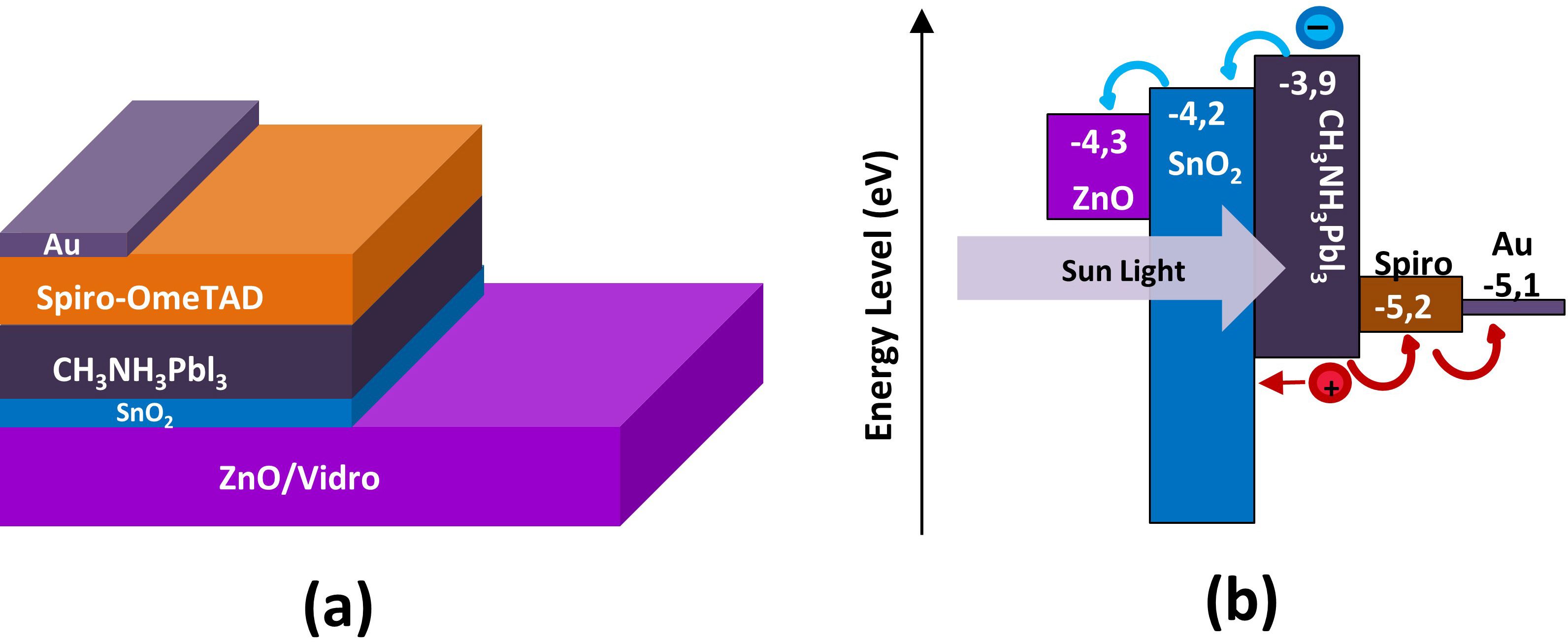
Another advantage of SnO2 for ETLs is that its conduction band falls between the Fermi levels of conductive oxides such as FTO, ITO and ZnO, generally used as transparent contact electrodes, and the conduction band of perovskite, favoring the transition of electrons caused by the absorption of photons by the active layer1111 Tao H, Wang H, Bai Y, Long H, Zhao H, Fu Q, et al. Effects of sputtering power of SnO2 electron selective layer on perovskite solar cells. J Mater Sci Mater Electron. 2019;30(13):12036-43.,1212 Kam M, Zhang Q, Zhang D, Fan Z. Room-temperature sputtered SnO2 as robust electron transport layer for air-stable and efficient perovskite solar cells on rigid and flexible substrates. Sci Rep. 2019;9(1):1-10.. Based on these factors, the energy levels of ZnO, SnO2 and of perovskite are presented in Figure 1, indicating the possible use of SnO2 as an ETL for PSCs.

(a) Scheme of the layer structure of a PSC; (b) Diagram of the band structure of a planar PSC prepared with sputtered SnO21111 Tao H, Wang H, Bai Y, Long H, Zhao H, Fu Q, et al. Effects of sputtering power of SnO2 electron selective layer on perovskite solar cells. J Mater Sci Mater Electron. 2019;30(13):12036-43..
For PSCs with SnO2 as the ETL, I-V curves show power conversion efficiencies (PCE) of ~10%, depending on the thickness1212 Kam M, Zhang Q, Zhang D, Fan Z. Room-temperature sputtered SnO2 as robust electron transport layer for air-stable and efficient perovskite solar cells on rigid and flexible substrates. Sci Rep. 2019;9(1):1-10.. If the SnO2 layer is very thin, the whole TCO surface is not covered and is therefore not totally effective in preventing electron-hole recombination. If the SnO2 layer is very thick, however, the resulting electrical resistance dissipates energy by the Joule effect77 Kavan L, Steier L, Gratzel M. Ultrathin buffer layers of SnO2 by atomic layer deposition: perfect blocking function and thermal stability. J Phys Chem C. 2017;121(1):342-50. http://dx.doi.org/10.1021/acs.jpcc.6b09965.
http://dx.doi.org/10.1021/acs.jpcc.6b099...
,1212 Kam M, Zhang Q, Zhang D, Fan Z. Room-temperature sputtered SnO2 as robust electron transport layer for air-stable and efficient perovskite solar cells on rigid and flexible substrates. Sci Rep. 2019;9(1):1-10.. In a study by Tao et al.2222 Tao H, Ma Z, Yang G, Wang H, Long H, Zhao H, et al. Room-temperature processed tin oxide thin film as effective hole blocking layer for planar perovskite solar cells. Appl Surf Sci. 2018;434:1336-43., the best results (PCE = 13.68%) were obtained for a SnO2 thickness of 18.9 nm.
In this study, SnO2/ZnO films were synthesised at room temperature on glass using RF magnetron sputtering (RFMS) to evaluate the morphological, optical and electrical properties as a function of the SnO2 thickness. The synthesis parameters of the ZnO films were chosen considering a high transmittance in the visible region and good electrical conductivity, so as to be suitable as a contact electrode in a solar cell. As ZnO is cheap and non-toxic, it has already been exploited in CIGS2323 Alhammadi S, Park H, Kim WK. Optimization of intrinsic ZnO thickness in Cu(In,Ga)Se2-based thin film solar cells. Materials. 2019;12(9):1365-80. solar cells. The choice of SnO2/ZnO is suggested by the low temperature needed for their synthesis and their properties being, in principle, compatible, especially regarding their refractive indices, as shown in Table 1.
Optical and electrical properties of SnO2 and ZnO33 Yang Y, Wu J, Guo P, Liu X, Guo Q, Liu Q, et al. Low-temperature sintered SnO2 electron transport layer for efficient planar perovskite solar cells. J Mater Sci Mater Electron. 2018;29(15):13138-47..
2. Experimental
Before deposition, the glass substrates were cleaned in detergent and distilled deionized water (DDW). Then they were washed sequentially in an ultrasonic bath of DDW, acetone, and alcohol, and finally dried by thermal blower. Both the SnO2 and the ZnO films were synthesised by RFMS at room-temperature. For ZnO, a ceramic ZnO target (of purity 99.999%) was used. The target-substrate separation was about 30 mm. Power (100 W) was applied at 13.56 MHz. Before deposition, the system was evacuated to a base pressure of 0.01 mTorr. For sputtering, 1.00 mTorr of argon was used for 30 min. Five ZnO/glass samples were synthesised under the same conditions. The ZnO films had thicknesses from 700 to 950 nm and sheet resistances of about 25 Ω/sq.
The SnO2 films were deposited using reactive RFMS at ambient temperature, the target being tin in a flow of oxygen. Four SnO2/ZnO/glass samples were produced. For the deposition of tin oxide the system was evacuated again to a base pressure of 0.01 mTorr, and argon gas fed in to a pressure of 1.00 mTorr and oxygen to a pressure of 2.00 mTorr. An applied power of 70 W was used for all the tin oxide depositions at times of 15 min, 30 min, 60 min and 90 min.
Optical properties were measured using an ultraviolet-visible near infrared spectrometer (Lambda 750, Perkin Elmer). Surface morphology of the SnO2 films was analysed by field emission scanning electron microscopy (MEV-FEG, Jeol JSM 7500F) and by atomic force microscopy (XE-100, Park Systems). Electrical properties were investigated by linear voltammetry using a potenciostat (128N Autolab) and the impedance spectroscopy was analised by Keysight E4980A.
3. Results and Discussion
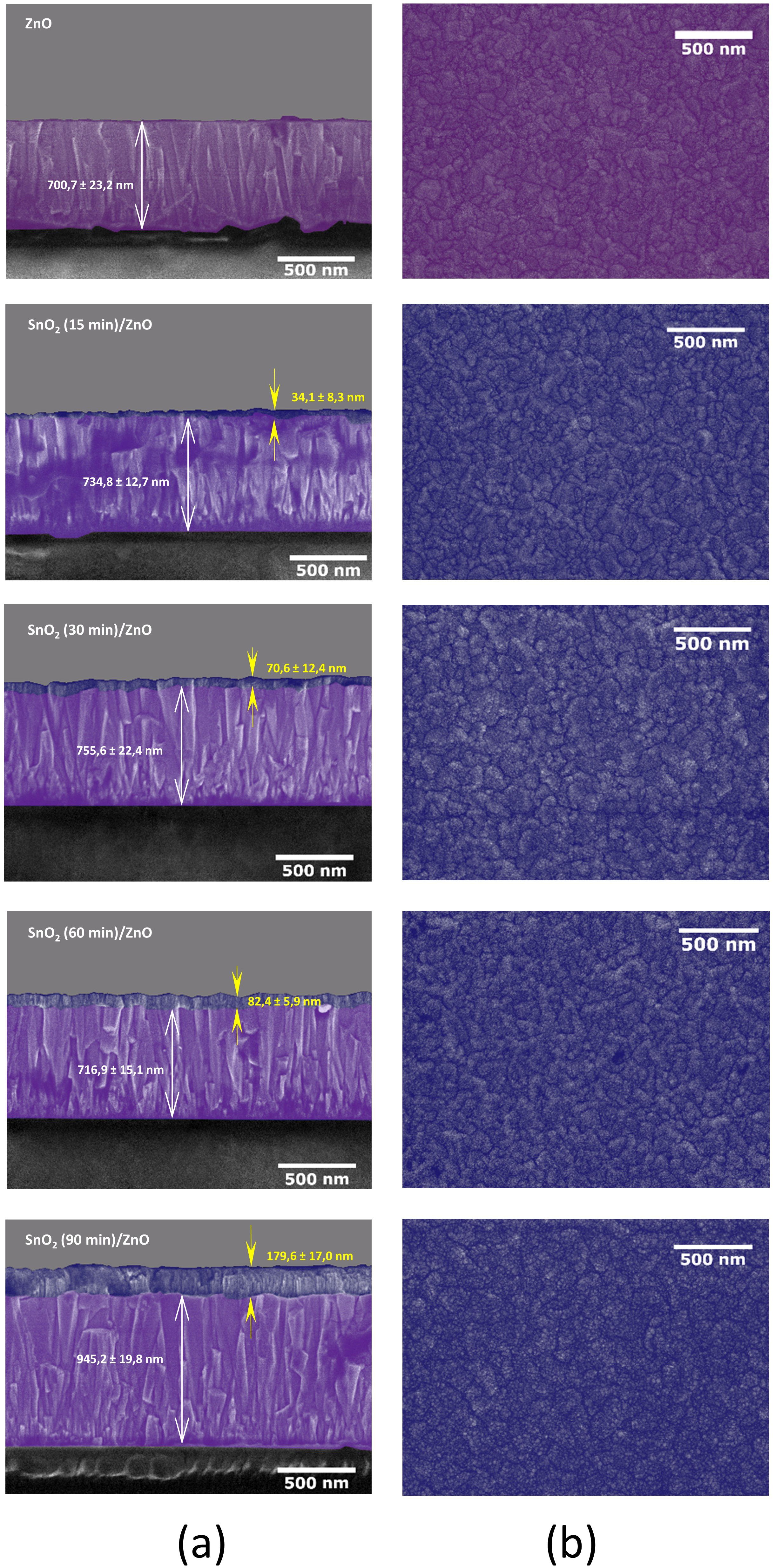
Figure 2 shows micrographs of cross-sections and surfaces of the ZnO and SnO2/ZnO films. In Figure 2a thicknesses of the SnO2 and ZnO layers are given for each sample. The results show that the thickness of the SnO2 varied from ~30 nm to ~180 nm, and the deposition rate was about 2 nm/min. According to Kam et al.1212 Kam M, Zhang Q, Zhang D, Fan Z. Room-temperature sputtered SnO2 as robust electron transport layer for air-stable and efficient perovskite solar cells on rigid and flexible substrates. Sci Rep. 2019;9(1):1-10., the thickness of the ETL significantly influences the optimization of the solar cell. Therefore, the morphological, optical, and electrical properties were studied as a function of the SnO2 layer thickness.

Micrographs of ZnO and SnO2/ZnO films obtained by MEV-FEG, (a) in cross-section and (b) top view, showing the evolution of the SnO2 with deposition time.
According to Figure 2a, the growth of the tin oxide layer is well-defined and conformal with the topography of the ZnO layer. Figure 2b shows the surfaces of the ZnO/glass and of the SnO2 deposited on ZnO/glass. Superimposed on the morphology of ZnO, there is the formation of smaller grains of SnO2, which increase the surface roughness.
Figure 3 shows AFM images (2 µm x 2 µm) of the same samples whose electron micrographs are shown in Figure 2. The root mean square roughness increases from 8.5 nm for the ZnO film to above 11 nm. This increase is caused by the presence of SnO2 grains superimposed on the ZnO morphology. These grains are typically around 50 nm, even for the thickest film (180 nm). These data indicate that the SnO2 exhibits a morphology similar to that found in other studies that use titanium dioxide (TiO2) or tin oxide as a compact layer1111 Tao H, Wang H, Bai Y, Long H, Zhao H, Fu Q, et al. Effects of sputtering power of SnO2 electron selective layer on perovskite solar cells. J Mater Sci Mater Electron. 2019;30(13):12036-43.,2424 Oliveira RRL, Albuquerque DAC, Cruz TGS, Yamaji FM, Leite FL. Measurement of the nanoscale roughness by atomic force microscopy: basic principles and applications. In: Bellitto V, editor. Atomic force microscopy: imaging, measuring and manipulating surfaces at the atomic scale. London: InTech; 2012. p. 147-74..

AFM images, of the ZnO and SnO2/ZnO films of different thickness. Also presented is a profile typical of the topography present in each AFM image.
Optical transmittance and reflectance, measured using UV-Vis-NIR spectroscopy, are presented in Figure 4. There is a fall in transmittance at about 370 nm (3.35 eV), where the absorption edge of ZnO lies2525 Swanepoel R. Determination of the thickness and optical constants of amorphous silicon. J Phys Earth. 1983;16:1214-22.. In addition, it is possible to observe that SnO2 did not significantly alter the optical properties in relation to the ZnO film, which is explained by the high gap energy of SnO2, which is between 3.6 eV and 4.1 eV2626 Barbe J, Tietze ML, Neophytou M, Murali B, Alarousu E, Labban AE, et al. Amorphous tin oxide as a low-temperature-processed electron-transport layer for organic and hybrid perovskite solar cells. ACS Appl Mater Interfaces. 2017;9(13):11828-36.. Even with the SnO2 layer, the transmittance in the visible is above 80%. A shift in the position of the interference extrema, caused by differences in the total thickness between samples, was observed.

Optical transmittance and reflectance spectra for the ZnO/glass and the SnO2/ZnO/glass samples.
The stability of the transmittance and reflectance values agrees with the literature values reported in Table 1. This result is significant, since SnO2 should not alter the optical properties of a solar cell, only acting as a selective charge carrier layer, increasing the electron-hole recombination time.
To allow comparison with other TCO materials, Figure 5 shows the transmittance and reflectance in the 200 nm to 1200 nm wavelength range, for ZnO/glass, SnO2/glass, SnO2/ZnO/glass and SnO2:F/glass (FTO). Data for FTO are presented since this materials is often used as a TCO in photovoltaic cells. A spectrum of the substrate is also included. Please note that the SnO2/ZnO/glass combination does not significantly alter the properties of ZnO, maintaining the transmittance around 80% and reflectance at about 15%. The transmittance of the SnO2/ZnO/glass combination is greater than that of the FTO curve in the visible region, indicating that SnO2 does not produce optical losses, even when part of a bilayer.

Transmittance and reflectance spectra in the UV-VIS of ZnO/glass, SnO2/ZnO/glass, SnO2/glass and FTO(SnO2:F)/glass samples.
Concerning desirable characteristics for electron excitation, SnO2 also shows potential because its energy gap is greater than that of ZnO. Consequently, ZnO will absorb photons for the excitation of electrons and the formation of electron-hole pairs at lower energies than SnO2. This may be observed in Figure 4, since the absorption region, corresponding to a region of reduced transmittance, is related to the level of the band energy of the gap of ZnO.
To evaluate the behavior of the SnO2/ZnO heterojunction, I-V curves were measured for the SnO2(60min)/ZnO/glass assembly, with one contact on the ZnO film and the other on the SnO2 film, in the dark, and illuminated with UV radiation. For this experiment, a mercury lamp without a protective bulb was used, emits UV radiation at wavelengths of 366 nm, 313 nm and 254 nm. The I-V curves, shown in Figure 6, show a Schottky behavior caused by a levelling of the Fermi levels, distorting the valence and conduction bands at the interface, giving rise to a potential barrier. Irradiation of the sample with UV radiation causes the current generated by the applied potential to increase, owing to the promotion of electrons from the valence to the conduction band. It can be observed, in the inset placed in Figure 6, the log(I)-V graph where we can observe that from 0.68 V on, the photogenerated current predominates in relation to the effects of the current injected into the system. This fact can be explained since the UV lamp promotes an increase in the population of charge carriers present in the conduction band of the ZnO.

Current-voltage measurements of SnO2(60min)/ZnO/glass samples in the dark and with UV illumination, inset Log(I)-V.
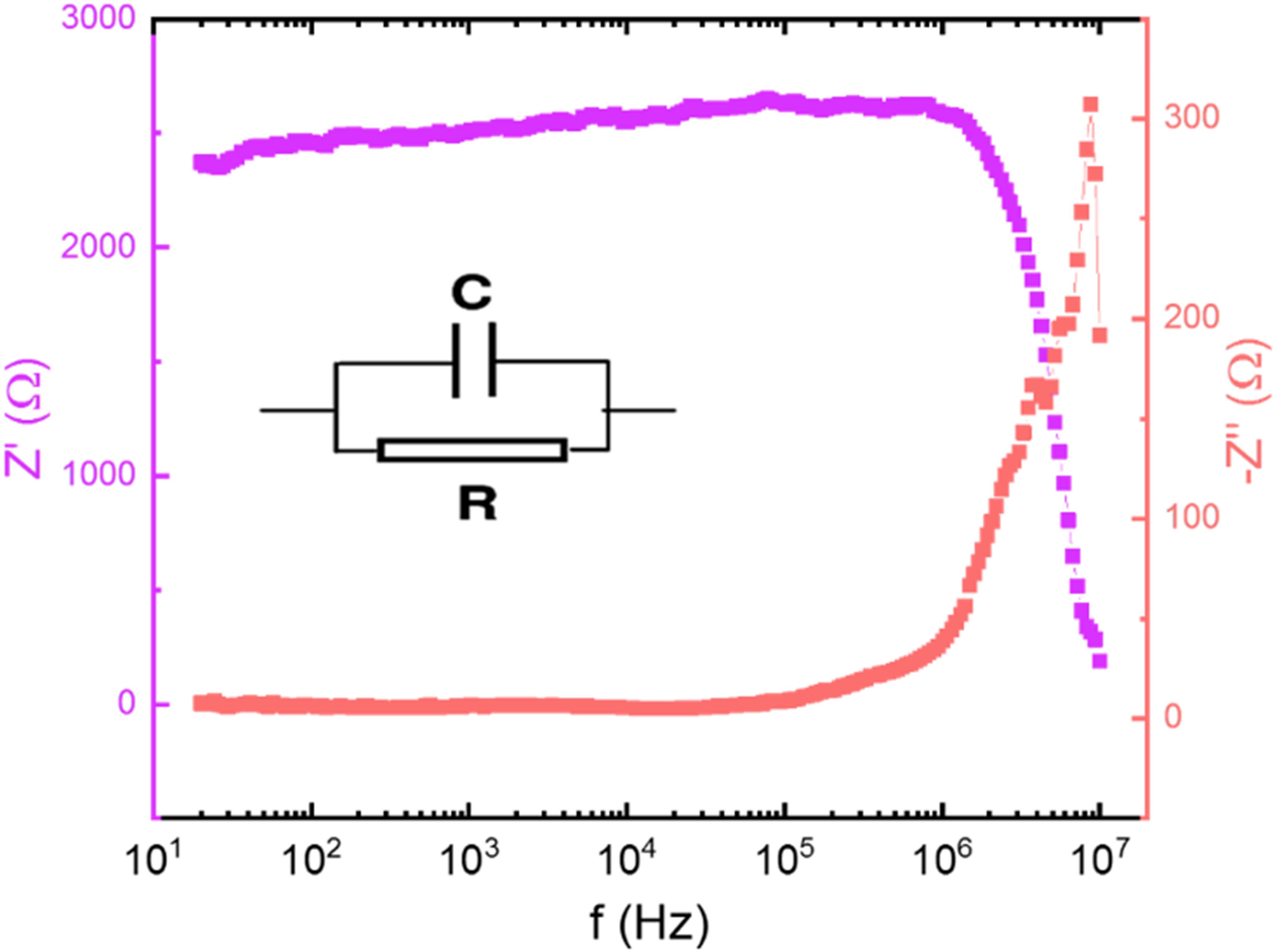
The studied heterojunction is composed of the conductive ZnO layer and the SnO2 layer that presents resistive behavior. To perform an analysis of the electrical properties of the studied heterojunction, a silver layer was deposited onto the SnO2 film and then impedance spectroscopy measurements were performed by applying 500 mV to the tips in contact with the ZnO and the silver layer (deposited on top of the SnO2). The real impedance (Z') and complex impedance (Z”) data were plotted in the Bode diagram shown in Figure 7 and it was found that the data varies only at high frequencies (>105 Hz), below this value the resistance and the capacitance of the material has an average of 2520 Ω and 1.12 nF, respectively. The inset to the graph shows the equivalent circuit of ZnO/SnO2 films.

4. Conclusions
An SnO2 ETL and a conductive ZnO layer were deposited by RF magnetron sputtering. The SnO2/ZnO system was analysed using Field Emission SEM, which allowed the evaluation of the development and growth of the SnO2 structure on ZnO. To verify the influence of SnO2 on ZnO the heterojunction was investigated using UV-Vis-NIR spectroscopy. The ZnO and SnO2/ZnO layers exhibited high transmittances (~80%) in the visible region, and showed that the SnO2 film did not alter the optical properties of the conductive oxide film. This is a promising result as it suggests the use of SnO2 on ZnO in the production of ETL layers used in perovskite solar cells and dye-sensitized solar cells.
5. Acknowledgements
The authors thank the Laboratório de Microscopia of the Instituto de Química, UNESP, Araraquara, for the electron microscope measurements and the use of the AutoLab, Laboratório Multiusuário LAMULT, ICTS, UNESP. The authors also thank the Brazilian agency CNPq (Proc. 555774/2010-4 and 301622/2012-4) for financial support. One of us (RR) acknowledges the financial suport of CAPES (1795290/2018). We thank the use of the Brazilian Nanotechnology Laboratory (LNNano) for the measurements of impedance spectroscopy.This study was financed in part by the Coordenação de Aperfeiçoamento de Pessoal de Nível Superior - Brasil (CAPES) - Finance Code 001.
6. References
-
1Sahli F, Werner J, Kamino BA, Bräuninger M, Monnard R, Paviet-Salomon B, et al. Fully textured monolithic perovskite/silicon tandem solar cells with 25.2% power conversion efficiency. Nat Mater. 2018;17(9):820-6.
-
2Chen Y, Meng Q, Zhang L, Han C, Gao H, Zhang Y, et al. SnO2-based electron transporting layer materials for perovskite solar cells: a review of recent progres. J Energy Chem. 2019;35:144-67.
-
3Yang Y, Wu J, Guo P, Liu X, Guo Q, Liu Q, et al. Low-temperature sintered SnO2 electron transport layer for efficient planar perovskite solar cells. J Mater Sci Mater Electron. 2018;29(15):13138-47.
-
4Xu Y, Liu T, Li Z, Feng B, Li S, Duan J, et al. Preparation and photovoltaic properties of perovskite solar cell based on ZnO nanorod arrays. Appl Surf Sci. 2016;388(3):89-96.
-
5Ke W, Zhao D, Grice CR, Cimaroli AJ, Ge J, Tao H, et al. Efficient planar perovskite solar cells using room-temperature vacuum-processed C60 electron selective layers. J Mater Chem A Mater Energy Sustain. 2015;3(35):17971-6.
-
6Chen JY, Chueh CC, Zhu Z, Chen WC, Jen AKY. Low-temperature electrodeposited crystalline SnO2 as an efficient electron-transporting layer for conventional perovskite solar cells. Sol Energy Mater Sol Cells. 2017;164:47-55.
-
7Kavan L, Steier L, Gratzel M. Ultrathin buffer layers of SnO2 by atomic layer deposition: perfect blocking function and thermal stability. J Phys Chem C. 2017;121(1):342-50. http://dx.doi.org/10.1021/acs.jpcc.6b09965
» http://dx.doi.org/10.1021/acs.jpcc.6b09965 -
8Chen Z, Yang G, Zheng X, Lei H, Chen C, Ma J, et al. Bulk heterojunction perovskite solar cells based on room temperature deposited hole-blocking layer: suppressed hysteresis and flexible photovoltaic application. J Power Sources. 2017;351:123-9.
-
9Sung YM. Deposition of TiO2 blocking layers of photovoltaic cell using rf magnetron sputtering technology. Energy Procedia. 2013;34:582-8.
-
10Jazmati AK, Abdallah B. Optical and structural study of ZnO Thin films deposited by rf magnetron sputtering at different thicknesses: a comparison with single crystal. Mater Res. 2018;21(3):1-6.
-
11Tao H, Wang H, Bai Y, Long H, Zhao H, Fu Q, et al. Effects of sputtering power of SnO2 electron selective layer on perovskite solar cells. J Mater Sci Mater Electron. 2019;30(13):12036-43.
-
12Kam M, Zhang Q, Zhang D, Fan Z. Room-temperature sputtered SnO2 as robust electron transport layer for air-stable and efficient perovskite solar cells on rigid and flexible substrates. Sci Rep. 2019;9(1):1-10.
-
13Gu PY, Wang N, Wu A, Wang Z, Tian M, Fu Z, et al. An azaacene derivative as promising electron‐transport layer for inverted perovskite solar cells. Journal Chemical Asian. 2016;11(15):2135-40.
-
14Said AA, Xie J, Zhang Q. Recent progress in organic electron transport materials in inverted perovskite solar cells. Small. 2019;15:1900854.
-
15Said AA, Xie J, Wang Y, Wang Z, Zhou Y, Zhao K, Gao WB, Michinobu T, Zhang Q. Efficient inverted perovskite solar cells by employing N‐type (D–A1–D–A2) polymers as electron transporting layer. Small. 2019;15:1803339.
-
16Choi J, Song S, Hörantner MT, Snaith HJ, Park T. Well-defined nanostructured, single-crystalline TiO2 electron transport layer for efficient planar perovskite solar cells. ACS Nano. 2016;10(6):6029-36.
-
17Alberti A, Smecca E, Sanzaro S, Bongiorno C, Giannazzo F, Mannino G, et al. Nanostructured TiO2 grown by low-temperature reactive sputtering for planar perovskite solar cells. ACS Applied Energy Materials. 2019;2(9):6218-29.
-
18Lee S-W, Bae S, Cho K, Kim S, Hwang J-K, Lee W, et al. Sputtering of TiO2 for high-efficiency perovskite and 23.1% perovskite/silicon 4‑terminal tandem solar cells. ACS Applied Energy Matererials. 2019;2(9):6263-8..
-
19Kim HI, Baek S-W, Choi M-J, Chen B, Ouellette O, Choi K, et al. Monolithic organic/colloidal quantum dot hybrid tandem solar cells via buffer engineering. Adv Mater. 2020;32(42):2004657.
-
20Liang L, Huang Z, Cai L, Chen W, Wang B, Chen K, et al. Magnetron sputtered zinc oxide nanorods as thickness-insensitive cathode interlayer for perovskite planar-heterojunction solar cells. ACS Appl Mater Interfaces. 2014;6(23):20585-9.
-
21Tainter GD, Hörantner MT, Pazos-Outón LM, Lamboll RD, Āboliņš H, Leijtens T, et al. Long-Range charge extraction in back-contact perovskite architectures via suppressed recombination. Joule. 2019;3(5):1301-13.
-
22Tao H, Ma Z, Yang G, Wang H, Long H, Zhao H, et al. Room-temperature processed tin oxide thin film as effective hole blocking layer for planar perovskite solar cells. Appl Surf Sci. 2018;434:1336-43.
-
23Alhammadi S, Park H, Kim WK. Optimization of intrinsic ZnO thickness in Cu(In,Ga)Se2-based thin film solar cells. Materials. 2019;12(9):1365-80.
-
24Oliveira RRL, Albuquerque DAC, Cruz TGS, Yamaji FM, Leite FL. Measurement of the nanoscale roughness by atomic force microscopy: basic principles and applications. In: Bellitto V, editor. Atomic force microscopy: imaging, measuring and manipulating surfaces at the atomic scale. London: InTech; 2012. p. 147-74.
-
25Swanepoel R. Determination of the thickness and optical constants of amorphous silicon. J Phys Earth. 1983;16:1214-22.
-
26Barbe J, Tietze ML, Neophytou M, Murali B, Alarousu E, Labban AE, et al. Amorphous tin oxide as a low-temperature-processed electron-transport layer for organic and hybrid perovskite solar cells. ACS Appl Mater Interfaces. 2017;9(13):11828-36.
Publication Dates
-
Publication in this collection
23 Aug 2021 -
Date of issue
2021
History
-
Received
20 Jan 2021 -
Reviewed
19 July 2021 -
Accepted
24 July 2021