
Abstract
This paper proposes a new topology of a 2-Stages Active Polyphase Filter (APPF) in MMIC GaAs technology. This new topology, named “radial”, allows a greater balancing of output signals phases and amplitudes, over the actual APPF’s at the state of the art. In this paper an ex-novo study is shown and synthesis formulas for the APPF are provided. The MMIC simulations in 1-5GHz bandwidth show a tunable Image Rejection Ratio (IRR) greater than 40dB, a worst case input/output matching of 7.8dB and a maximum insertion loss of 10.8dB. By comparison with the tandem topology, as will be shown in the following, the radial one allows a significant improvement in the electrical performances.
Index Terms
Active Polyphase Filter; Tunable Polyphase Filter; monolithic; excitation mode; image reject receiver
I. introduction
Actual mobile telecommunication systems have greatly increased the demand for wideband circuits to transmit and receive a great amount of data while maintaining small dimensions and low cost. Electronic tunability and filtering of the operating frequency is now day a must, and this requirement, together with the need of small dimensions of the system, force many designers to avoid dedicate off-chip filtering sections. In fact, filters, considered as standalone circuits, are quite bulky and costly: for this reason, now day all the filtering is attempted to be realized at chip level.
A common problem in such wideband receivers is to cancel at the greatest extent the image frequency, and one solution to reduce the filtering problem is to employ Image Rejection Mixers (IRM) 11 S. Maas: "Microwave Mixers", Artech House, Second Edition, 1993. Such mixers need quadrature Local Oscillator (LO) signals, and the IRR achievable by such IRM's is directly dependent by the quality of the quadrature and amplitude unbalancing of these LO signals. So, high quality and wideband quadrature signals generation is a very important requirement in any modern telecommunication systems22 A.A. Abidi: "Direct-Conversion Radio Transceivers for Digital Communications", IEEE Journal of SSC, Vol. 30, N.12, Dec. 1995, p: 1399-14103 Markus Ortner, H.P. Forstner, Ludger Verweyen and Timm Ostermann "A Fully Integrated Homodyne Downconverter MMIC in SiGe:C for 60 GHz Wireless Applications”, IEEE SiRF, 2011.-44 B. Schlecker, M. Ortmanns, J. Anders, G. Fartner: "Novel electronics for high-speed FM-AFM in life science applications”, European Conference on Circuit Theory and Design, p. 1–4, 2013., and electronic tunability is a great desired possibility.
However, modern telecommunications systems are not the only who need signal quadrature: standard communications systems, as those used by Amateurs Radio, still need good quadrature signals for sideband selection and generation [5],[6]55 Donald E. Noorgaard: "The Phase-Shift Method of Single-Sideband Signal Reception”, Proc. IRE, vol. 44, n.1, pp. 1735-1743, December 1956.66 M.J. Gingell: "Single Sideband Modulation using Sequence Asymmetric Polyphase Networks", Electrical Communication, Vol 48, n.1,2, 1973, p: 21-25..
For all these applications, the polyphase filter77 Jouni Kaukovuori, Kari Stadius, Jussy Ryynänen and Kari A. I. Halonen: "Analysis and Design of Passive polyphase Filters”, IEEE Transactions on Circuits and Systems, vol. 55, NO. 10, pp. 3023-3037, November 2008.8 F. Behbahani, Y. Kishigami, J. Leet, A.A. Abidi: "CMOS Mixer and Polyphase Filters for Large Image Rejection", IEEE Journals of SSC, Vol. 3, N.6, June 2001, p: 873-8869 T. Hornak: "Using Polyphase Filters as Image Attenuators", RF Design, Vol. 13, N. 2, June 2001, p: 26-34-1010 Yang Jiao, Zhizhong Huang, Li L: "CMOS analog polyphase filters for use in bluetooth systems", 9th International Conference on Solid-State and Integrated-Circuit Technology, 2008, p:1677-1680 , is eventually a valid candidate due its wideband operation and it is well suited to be simply integrated in MMIC technologies; hence, it is very attractive for a lot of miniaturized and cost effective electronic systems.
Furthermore, it must be considered that the polyphase filter can be used as a phase shifter 1111 H. Erkens, R. Wunderlich, S. Heinen: "A Low-Cost, High Resolution, 360° Phase/Gain Shifter in SiGe BiCMOS”, IEEE Topical Meeting on Silicon Monolithic Integrated Circuits in RF Systems, 2009, San Diego, CA, p:1-4: by varying the outputs amplitudes, for example using Variable Gain Amplifiers (VGA’s), and combining them it’s possible to change phase of the output signal. .
Unfortunately, at the actual state of the art, multistage APPF’s are realized in tandem topology, which are topologically limited by a low balancing of phases and amplitudes of the output signals.
In order to overcome such drawback, in this paper we propose a new PPF topology with synthesis formulas and an useful application example to estimate the powerful of the proposed solution.
This paper is organized as follows:
In Section II the analysis of PPF is briefly exposed, giving expressions for input and output differential impedances. In Section III, the strategy used to select the tuning element is reported. In Section IV, the design of the radial and tandem topologies of the APPF 1-5GHz in GaAs technology is shown. Finally, in Section V we report the conclusions of this work.
II. The Polyphase Filter Solution
The polyphase filter (PPF) is an n-port electric network composed by a series connection of multiple stages of RC sub-networks, each of them is a ring of resistors and capacitors arranged alternately in a closed loop. In the simplest case, the polyphase filter has 4 inputs and 4 outputs (4I/O), but in the most general case it can have n-inputs and n-outputs. For example, a one stage 4 I/O polyphase filter can be seen in Figure 1Figure 1: the outputs O1…O4 can be considered as 4 unbalanced ones, otherwise as a couple of balanced (or differential) ports O1-O3 and O2-O4. Between each port and the nearest ones there is a 90° phase difference [1]; for example, the signal taken between the ground and the port O1 (O2) and the signal taken between the ground and the port O2 (O3) there is a phase shift of 90°. Hence, by taken as reference for instance the signal between the ground and the port O1, the signals taken between the ground at the ports O2 , O3 and O4 have respectively of 90, 180° and 270°: It means that ports O1 and O3 and the ports O2 and O4 are couples of differential ports and a phase shift of 90° exists between such two couples of differential ports [7]. The main application of the PPF in Figure 1 is that to generate 4 quadrature signals at the outputs, a required function in an image reject receiver or in a SSB modulator for example.
An innovative design approach is proposed in this paper, it is based on a "radial topology", which does not introduce phase and amplitude imbalances. The physical layout can be considered as a design requirement as will be described in this paper. APPF have been implemented in CMOS technology, 1212 F. Haddad, W. Rahajandraibe, L Zaid, O. Frioui and R. Bouchakour "Radio Frequency Tunable Polyphase Filter Design”, 16th IEEE International Conference on Electronics, Circuits, and Systems, 2009, p:21-2413 M. Kaltiokallio, J. Ryynnen: "A 1 to 5GHz adjustable active polyphase filter for LO quadrature generation", IEEE Radio Frequency Integrated Circuits Symposium (RFIC), 2011, Baltimore, MD, p:1- 4-1414 G. Souliotis, F. Plessas, F. Liakou & M. Birbas "A 90 nm CMOS 15/60 GHz frequency quadrupler”, International Journal of Electronics, Volume 100, Issue 11, 2013, pages 1529-1545. but until now never in GaAs technology. The range 1-5GHz is easily covered in CMOS technology which is inexpensive and the circuit can be included on the same die with other blocks. Good values of IRR are also achieved with more stages. However, in this project, the GaAs technology has been considered because it is a high reliability process with low losses in the microwave region and a low cost process respect Silicon process especially for relatively small volume production 77 Jouni Kaukovuori, Kari Stadius, Jussy Ryynänen and Kari A. I. Halonen: "Analysis and Design of Passive polyphase Filters”, IEEE Transactions on Circuits and Systems, vol. 55, NO. 10, pp. 3023-3037, November 2008.15 E. Cohen, "Microwave GaAs FETs: Reliability and reproducibility”, IEEE International Solid-State Circuits Conference, 18-20 Feb. 1976, Philadelphia, USA, p. 174.16 R. E. Lundgren, G. O. Ladd, "Reliability Study of Microwave GaAs Field-Effect Transistors”, 16th Annual Reliability Physics Symposium, 1978. San Diego, USA, pp. 255 – 260.17 J. Magarshack, "Microwave Integrated Circuits on GaAs”, 12th European Microwave Conference, Helsinki, Finland , 13-17 Sept. 1982, pp. 5 - 15.-1818 B.K. Schwitter, A. E. Parker, A. P. Fattorini, S. J. Mahon, M. C. Heimlich, "Study of Gate Junction Temperature in GaAs pHEMTs Using Gate Metal Resistance Thermometry”, IEEE Transactions on Electron Devices, Vol. 60 , Issue 10, IEEE, 2013, pp.3358 – 3364.. The GaAs APPF proposed in this paper has the same performances in terms of covered bandwidth, insertion loss, matching and IIR, but it has many advantages compared to CMOS APPF mentioned above; it can be developed for working at higher frequencies thanks first to GaAs which has less parasitic capacitances and higher charge carriers drift velocity 1919 S. E. Gunnarsson, C. Karnfelt, H. Zirath, R. Kozhuharov, D. Kuylenstierna, C. Fager, A. Alping, "Single-Chip 60 GHz Transmitter and Receiver MMICs in a GaAs mHEMT Technology”, IEEE MTT-S International Microwave Symposium Digest, 11-16 June 2006, San Francisco, CA, pp. 801 – 804.20 C. Zhe, S. Rea,W. Hui, B. Alderman, Z. Bo, F. Yong, "A power combined amplifier module in W-band”, 6th UK Europe, China Millimeter Waves and THz Technology Workshop (UCMMT), 2013, 9-11 Sept. 2013, Rome, Italy, p.1.-2121 J. J. Komiak, P. M. Smith, K. H. G. Duh, K.H.G. ; D. Xu, P. C. Chao, "Metamorphic HEMT Technology for Microwave, Millimeter-Wave, and Submillimeter-Wave Applications", IEEE Compound Semiconductor Integrated Circuit Symposium (CSICS), 13-16 Oct. 2013, Monterey, CA, pp. 1-4.. Furthermore, there are other two advantages that should be considered, GaAs APPF can work in extreme temperature conditions thanks to larger GaAs band gap and it is radiation resistant thanks to absence of gate oxide 2222 J. Würfl, "Recent advances in GaAs devices for use at high temperatures", High-Temperature Electronic Materials, Devices and Sensors Conference, 22-27 Feb 1998, San Diego, CA, pp. 106 – 116.23 R. Narasimhan, L. P. Sadwick, R. J. Hwu, "Enhancement of high-temperature high-frequency performance of GaAs-based FETs by the high-temperature electronic technique”, IEEE Transactions on Electron Devices , Vol. 46, Issue 1, pp. 24 – 31. -2424 L. Ji, C. Kuan-Jung, H. Hu, J. B. Bernstein, "Temperature dependence of Ron,sp in silicon carbide and GaAs Schottky diode”, proc. of 40th Annual Reliability Physics Symposium Proceedings, IEEE, 2002, pp. 425 – 426., for this reasons it can be used for spatial and military applications.

Fig.1. One stage, 4-Inputs/Outputs (4I/O) passive Polyphase Filter, loads ZL are included.
III. Analytical Approach and Derivation of the Formulas
A. Excitation Mode
There are two ways to excite network in Figure 1: in the first one, named “Type I”, only one half of the inputs are excited, while with second way, named “Type II”, all the 4 inputs are excited. These excitations modes can be seen in Figures 2 and 3.

Fig.2. "Type I” excitation.
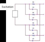
Fig.3. "Type II” excitation.
With “Type I” excitation, the first and third inputs are connected to the generator, i.e. such inputs have 180° phase difference between them, while with “Type II” excitation the first input with the second one and the third input with the fourth one are connected together, so that it result in a two input network. The choice of excitation mode determines the characteristics of the differential output signals, as we will show in the following.
B. Transfer Functions
Considering a one stage PPF as those in Figure 1 and that each output is connected to the same load, the two differential output signals are the following expressions (1) and (2):

(1)

(2)
where ΔViout and Δqout are differential output signals while ΔViin and ΔVqin are differential input signal and Zl is load impedance of each output. The pole angular frequency of one stage polyphase filter is 1/(R1*C1). From the above equations we obtain, for “Type I” excitation, the relation

(3)

(4)
With simple circuit analysis used above for (1)-(4), it’s possible to calculate transfer functions of multi-stages networks. The previous transfer functions show that with "Type I” excitation the phase difference between the two differential output signal is 90° for all frequencies and load impedances, but they have same amplitude only at each RC pole; instead, while with "Type II” excitation the phase difference between the two differential output signals is 90° only at each RC pole but they have same amplitude for all frequencies and load impedances. Also, network with "Type II” excitation has the insertion loss about 3 dB less than that with "Type I” excitation [1]. The theory exposed above is now applied to a two stage APPF. A two stage type II polyphase filter is depicted in Fig. 4.
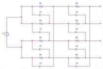
With simple circuit analysis used above for (1)-(4), it’s possible to calculate transfer functions of multi-stages networks. The previous transfer functions show that with "Type I” excitation the phase difference between the two differential output signal is 90° for all frequencies and load impedances, but they have same amplitude only at each RC pole; instead, while with "Type II” excitation the phase difference between the two differential output signals is 90° only at each RC pole but they have same amplitude for all frequencies and load impedances. Also, network with "Type II” excitation has the insertion loss about 3 dB less than that with "Type I” excitation [1]. The theory exposed above is now applied to a two stage APPF. A two stage type II polyphase filter is depicted in Fig. 4.
Fig.4. Two stage type II excitation model for polyphase filter.
The phase difference between differential ports can be seen in Figures. 5 and 6 for both excitation modes; we refer to two stages PPF where poles are indicated by f1 and f2, being f1 the pole of first stage and f2 the pole of second stage, i.e:

(5)

"Type I” excitation.
Fig.5. Phase difference between differential output signals,

Fig.6. Phase difference between differential output signals,
"Type II” excitation.
C. Differential Impedances
The overall loss of polyphase filter is composed of two terms: the intrinsic one, and that due to input and output load impedances. Let us indicate withZSdiff and ZLdiff the source and load differential impedance, and with Z?diff and ZOUTdiff the input and output differential impedances. As an example, for the differential impedances the equivalent circuit at the input can be seen in Figure 7.
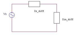
Fig.7. Effect of source termination.
Clearly, in Figure 6 we consider the effect of differential impedance at input; of course, to consider the effect of load termination ZSdiff andZ?diff must be replaced with ZOUTdiff andZLdiff.
Calculating input and output differential impedances for both excitation types, we obtain:

(6)

(7)

for “Type I” excitation, and
(8)

(9)
for "Type II” excitation: these expressions are used for input/output matching.
D. Image Reject Ratio, IRR
IRR is the Image Reject Ratio, i.e. it is the ratio between the desired and image signals. IRR depends of the phase and amplitude errors between two differential signals and its relation with them is shown in the following equation derived from Norgaard [5]:

(10)
where ΔTheta is phase error respect pi/2, while Abat is amplitude ratio between two differential signals, i.e:

(11)

(12)
The amplitude ratio Abat is obtained by the ratio between the differential output signals’ modulus, the (11) can be write as in (13) :

(13)
where ΔVi and ΔVq are defined in (14) and (15).

(14)

(15)
Defining the IRR parameter in log scale, yelds:

(16)
The in-frequency behavior of the IRR in dB Magnitude can be shown as in Fig. 8.
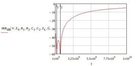
Fig.8. IRR vs frequency
An useful information on the character of the proposed circuit can be obtained by observing the behavior of the two parameters from which the IRR depends (), while changing the frequency of the input signal. As a main feature, there is the complete independence of the amplitude ratio to the frequency of the signal, as shown inFig. 9. The phase difference with respect the 90° phase shift between the two signals is an important figure of merit. Such value should be 0° ( or 180° ) for signals whose phase shift must be 90°; depending on the order into the expression (12). In Fig. 10, the behavior of is plotted and the operative bandwidth can be observed to have a like constant behavior with a low ripple. The two differential output signals have the same modulus at any frequency but a phase difference between each other of 90° only at the poles’ frequency.
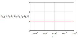
Fig.9. Amplitude ratio vs frequency.

Fig.10. Phase difference ∆θ with respect the 90° phase shift
The IRR is maximized when two differential signals have 90° phase difference each other and same amplitude, as shown in Figure 11

Fig.11. Graphic of the IRR vs. Aball and ∆θ.
Analyzing the expression of the IRR is evident that under ideal conditions, which are and ( or 180° ), the IRR tends approaching the infinity.
IV. Application: GaAs Active Polyphase Filter
A. Technology
The GaAs technology was used to realize the project of a 2-Stage 4I/O APPF. The technology chosen for the project was GaAs mainly because it is a high reliability and low cost process for relatively small volume production.
The design is based on a numerical simulation of the device with several iterative optimization. Since the simulation has been performed in a factory provided ambient, by employing the library of transistors, microstrips, lumped elements and substrate provided by the foundry, we can consider these result with a nice grade of reliability.
There are two ways to vary the poles in each stage: first, using a FET as a variable transconductance and second, using the FET as a variable capacitance. Our choice was the first and we employed a European Foundry.
Figures. 12 shows the transconductance vs. the VGS control voltage ( hereinafter named Vtune ) for a FET with 30 um gate periphery. The FET was connected in parallel to each resistors of the polyphase network, so that we can vary the poles, and consequently the IRR curve translates inside the request band, simply by varying the VGS voltage.
The JFET channel conducts at Vgs=0 because it is a depletion device, as the voltage became more negative the channel starts to close and the resistance increases reaching an opened channel at a voltage of -1V.

Fig.12. Transconductance FET vs VGS.
The FET works into ohmic region where it behaves as a resistor with the following approximated expression (17).

(17)
where ρ is the resistivity of the channel, L is the length, W is the width while t is the thickness of the channel . The transconductance can be approximated by the following expression (18):

(18)
In order to compute the transconductance in the factory-provided simulation ambient, the setup shown in Fig. 13 has been implemented. The FET’s transconductance behavior in the bandwidth has been measured through the Agilent ADS software, by employing the vendor’s library model.

Fig.13. Simulation set-up for measuring the FET’s transconductance.
B. Device Design: The Importance of Radial Structure
A schematic of both topologies we have considered, the "modular structure” and the "radial structure”, are given in Figures. 14and 15. The principal difference in realizing the physical layout of the "radial structure” is the complete symmetrical disposition of components and transmission lines. This is an important issue in the device performances. By employing the radial design, the device compactness can be ensured with the minimum encumbrances as a design requirement, from the beginning of the design. This approach could ensure the needed compactness while ensuring the minimum phase error without phase and amplitude imbalances. The spatial arrangement of components can be evaluated in the first step of the design starting by considering the electrical length of the transmission lines and their impact on the physical lengths.

Fig.14. The Modular Structure.

Fig.15. The Innovative Radial Structure.
The design starts with the choice of an excitation type; the "Type II” excitation mode was our choice because it presents a loss about 3 dB less than a "Type I” excitation way. Next step was the choice of a number of stages to cover the entire band 1-5 GHz: two stages were necessary, as shown in Figures. 16.

Fig.16. Schematic of the proposed Tunable Active Polyphase Filter.
In each stage different poles were chosen to obtain maximum bandwidth. Performing only a circuit analysis it is not evident the effects due to the network’s physical asymmetry, while with RF analysis we understand that the layout of the structure is decisive on the whole electrical performances. To maintain the symmetry of the network a new structure was designed named "RADIAL STRUCTURE”. This structure has two concentric stages as can be seen in the layout of Figure 17. In the left side of the layout, it can be seen the DC power supply line "IN+” and "IN- and the DC input control voltage Vtune, at top and bottom the inputs and left and right the outputs; its dimensions are 1350 um x 1830 um. For comparison, the modular structure layout is shown in Figures. 18Figure 18. It can be seen from Figure 12 that the band of "RADIAL” layout is greater than "MODULAR” one.

Fig.17. “RADIAL STRUCTURE” layout of a Tunable Active Polyphase Filter.

Fig.18. "MODULAR STRUCTURE” layout of a Tunable Active Polyphase Filter.
C. Simulation Results
Radial and Modular circuits were simulated with Agilent ADS (Advanced Design System) software and the IRR performances have been investigated. By using the theoretical equations given previously, these IRR values correspond to a phase error of about 0.5° and . As shown in Fig. 19, the IRR of the radial structure reaches a value of -45dB at 1GHz for Vtune = -1V and it reaches a value of -45dB at 5GHz for Vtune = 0V, consequently the phase error reaches a value of 0.5°; this value is obtained, varying Vtune from 0V to -1V, into the entire range of frequencies 1 - 5 GHz. The insertion losses has also been investigated and the dependence to Vtune and frequency is reported in Figure. 20.

IRR for modular layout (red line) and radiallayout (blue line) for Vtune =-1V and Vtune=0V.
Fig.19. IRR for modular layout (red line) and radial layout (blue line) for Vtune =-1V and Vtune=0V.
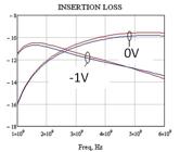
Insertion loss of a radial structure for both differential outputs O1-O3 (red line) and O2-O4 (blue line) for Vtune =-1V and Vtune=0V.
Fig.20. Insertion loss of a radial structure for both differential outputs O1-O3 (red line) and O2-O4 (blue line) for Vtune =-1V and Vtune=0V.
In the following Figures. 21 and 22 the reflection scattering parameter are plotted respectively for control voltage Vtune = -1V and Vtune = 0V, relative to the worst case among all possible VGS.

Fig.21. S11 dB Magnitude at all ports for control voltage Vtune= -1V.

Fig.22. S11 dB Magnitude at all ports for control voltage Vtune= 0V.
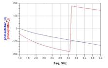
The phase of both differential signals versus Vtune is shown in Fig. 23 and 24, from which is evident that signals have a phase difference of 90° at 1 GHz for Vtune = -1V and at 5 GHz for Vtune = 0V.

Phase (deg) vs Frequency (GHz) behavior of the signal O1-O3 (blue) and O2-O4 (red) for Vtune=-1V
Fig.23. Phase (deg) vs Frequency (GHz) behavior of the signal O1-O3 (blue) and O2-O4 (red) for Vtune=-1V
Phase (deg) vs Frequency (GHz) behavior of the signal O1-O3 (blue) and O2-O4 (red) for Vtune= 0V
Fig.24. Phase (deg) vs Frequency (GHz) behavior of the signal O1-O3 (blue) and O2-O4 (red) for Vtune= 0V
By analyzing the circuit as formed by lumped elements and considering the frequency range of 1 – 5 GHz we cannot realize that the performance of polyphase filter are also influenced by the symmetry of the network; the radial topology can also be applied at higher frequencies, such as 60/70 GHz for radar applications thanks its symmetry.
At high frequency the different path between the elements (C and R) can change the amplitude and the phase of the output signals leading a differential signals which have no more a difference phase of 90°.
The proposed device offers a global performance increase over the classical poliphase filters [6-13], such as IRR value and matching that can not be obtained in a classical Modular layout configuration.
V. Conclusions
In this paper, PPF technology has been investigated, in order to respond to the growing demand for very wideband and narrow encumbrance telecommunication devices, such as 4 quadrature signals generators and Phase Shifters, suitable for circuits able to transmit a greater amount of data in line with the new requirements of the modern telecommunication devices. The PPF at the actual state of the art are only the Tandem kind, which are limited by a low balancing of phases and amplitudes of the output signals. We have shown a solution to overcome such drawback, by proposing a new PPF topology with direct synthesis formulas for the device design.
An example of application has been described and compared to the classical solution. The design and performance of a GaAs MMIC 2-Stages 4I/O Tunable APPF working in 1-5GHz bandwidth has been documented. Two types of layout have been proposed, one being the classical tandem connection of stages, and a new one named "radial” which permits a higher symmetry in the signal paths. The performed simulations show that the radial layout for the Tunable APPF has an output signals with a 0.5° phase unbalance, with an 8 dB of worst case matching and a 16 dB of maximum insertion loss. The tunability is obtained by varying the gate voltage of FET’s inside the range 0;-1V, allowing to cover the full 1-5GHz bandwidth.
REFERENCES
-
1S. Maas: "Microwave Mixers", Artech House, Second Edition, 1993
-
2A.A. Abidi: "Direct-Conversion Radio Transceivers for Digital Communications", IEEE Journal of SSC, Vol. 30, N.12, Dec. 1995, p: 1399-1410
-
3Markus Ortner, H.P. Forstner, Ludger Verweyen and Timm Ostermann "A Fully Integrated Homodyne Downconverter MMIC in SiGe:C for 60 GHz Wireless Applications”, IEEE SiRF, 2011.
-
4B. Schlecker, M. Ortmanns, J. Anders, G. Fartner: "Novel electronics for high-speed FM-AFM in life science applications”, European Conference on Circuit Theory and Design, p. 1–4, 2013.
-
5Donald E. Noorgaard: "The Phase-Shift Method of Single-Sideband Signal Reception”, Proc. IRE, vol. 44, n.1, pp. 1735-1743, December 1956.
-
6M.J. Gingell: "Single Sideband Modulation using Sequence Asymmetric Polyphase Networks", Electrical Communication, Vol 48, n.1,2, 1973, p: 21-25.
-
7Jouni Kaukovuori, Kari Stadius, Jussy Ryynänen and Kari A. I. Halonen: "Analysis and Design of Passive polyphase Filters”, IEEE Transactions on Circuits and Systems, vol. 55, NO. 10, pp. 3023-3037, November 2008.
-
8F. Behbahani, Y. Kishigami, J. Leet, A.A. Abidi: "CMOS Mixer and Polyphase Filters for Large Image Rejection", IEEE Journals of SSC, Vol. 3, N.6, June 2001, p: 873-886
-
9T. Hornak: "Using Polyphase Filters as Image Attenuators", RF Design, Vol. 13, N. 2, June 2001, p: 26-34
-
10Yang Jiao, Zhizhong Huang, Li L: "CMOS analog polyphase filters for use in bluetooth systems", 9th International Conference on Solid-State and Integrated-Circuit Technology, 2008, p:1677-1680
-
11H. Erkens, R. Wunderlich, S. Heinen: "A Low-Cost, High Resolution, 360° Phase/Gain Shifter in SiGe BiCMOS”, IEEE Topical Meeting on Silicon Monolithic Integrated Circuits in RF Systems, 2009, San Diego, CA, p:1-4
-
12F. Haddad, W. Rahajandraibe, L Zaid, O. Frioui and R. Bouchakour "Radio Frequency Tunable Polyphase Filter Design”, 16th IEEE International Conference on Electronics, Circuits, and Systems, 2009, p:21-24
-
13M. Kaltiokallio, J. Ryynnen: "A 1 to 5GHz adjustable active polyphase filter for LO quadrature generation", IEEE Radio Frequency Integrated Circuits Symposium (RFIC), 2011, Baltimore, MD, p:1- 4
-
14G. Souliotis, F. Plessas, F. Liakou & M. Birbas "A 90 nm CMOS 15/60 GHz frequency quadrupler”, International Journal of Electronics, Volume 100, Issue 11, 2013, pages 1529-1545.
-
15E. Cohen, "Microwave GaAs FETs: Reliability and reproducibility”, IEEE International Solid-State Circuits Conference, 18-20 Feb. 1976, Philadelphia, USA, p. 174.
-
16R. E. Lundgren, G. O. Ladd, "Reliability Study of Microwave GaAs Field-Effect Transistors”, 16th Annual Reliability Physics Symposium, 1978. San Diego, USA, pp. 255 – 260.
-
17J. Magarshack, "Microwave Integrated Circuits on GaAs”, 12th European Microwave Conference, Helsinki, Finland , 13-17 Sept. 1982, pp. 5 - 15.
-
18B.K. Schwitter, A. E. Parker, A. P. Fattorini, S. J. Mahon, M. C. Heimlich, "Study of Gate Junction Temperature in GaAs pHEMTs Using Gate Metal Resistance Thermometry”, IEEE Transactions on Electron Devices, Vol. 60 , Issue 10, IEEE, 2013, pp.3358 – 3364.
-
19S. E. Gunnarsson, C. Karnfelt, H. Zirath, R. Kozhuharov, D. Kuylenstierna, C. Fager, A. Alping, "Single-Chip 60 GHz Transmitter and Receiver MMICs in a GaAs mHEMT Technology”, IEEE MTT-S International Microwave Symposium Digest, 11-16 June 2006, San Francisco, CA, pp. 801 – 804.
-
20C. Zhe, S. Rea,W. Hui, B. Alderman, Z. Bo, F. Yong, "A power combined amplifier module in W-band”, 6th UK Europe, China Millimeter Waves and THz Technology Workshop (UCMMT), 2013, 9-11 Sept. 2013, Rome, Italy, p.1.
-
21J. J. Komiak, P. M. Smith, K. H. G. Duh, K.H.G. ; D. Xu, P. C. Chao, "Metamorphic HEMT Technology for Microwave, Millimeter-Wave, and Submillimeter-Wave Applications", IEEE Compound Semiconductor Integrated Circuit Symposium (CSICS), 13-16 Oct. 2013, Monterey, CA, pp. 1-4.
-
22J. Würfl, "Recent advances in GaAs devices for use at high temperatures", High-Temperature Electronic Materials, Devices and Sensors Conference, 22-27 Feb 1998, San Diego, CA, pp. 106 – 116.
-
23R. Narasimhan, L. P. Sadwick, R. J. Hwu, "Enhancement of high-temperature high-frequency performance of GaAs-based FETs by the high-temperature electronic technique”, IEEE Transactions on Electron Devices , Vol. 46, Issue 1, pp. 24 – 31.
-
24L. Ji, C. Kuan-Jung, H. Hu, J. B. Bernstein, "Temperature dependence of Ron,sp in silicon carbide and GaAs Schottky diode”, proc. of 40th Annual Reliability Physics Symposium Proceedings, IEEE, 2002, pp. 425 – 426.
Publication Dates
-
Publication in this collection
June 2015
History
-
Received
02 July 2014 -
Reviewed
14 July 2014 -
Accepted
29 Jan 2015

 Thumbnail
 Thumbnail
 Thumbnail
 Thumbnail
 Thumbnail
 Thumbnail
 Thumbnail
 Thumbnail
 Thumbnail
 Thumbnail
 Thumbnail
 Thumbnail
 Thumbnail
 Thumbnail
 Thumbnail
 Thumbnail
 Thumbnail
 Thumbnail


