
Abstract
An UWB antenna design with finite ground plane approach and multiple notches is reported. The antenna design provided a 10 dB bandwidth in excess of 8 GHz with better return loss characteristics. The antenna implemented in FR4 substrate, is compact and cost effective. The measured antenna parameters are in agreement with simulation.
Index Terms
Finite ground plane; Microstrip patch antenna; multiple notches ultra wide band
introduction
High data rate wireless transmission is the current requirement for many applications. The lower frequency bands used by various communication networks are over-crowded and hence channel allocation for large amount of data transmission has become difficult. Ultra Wide Band (UWB) technology operating in the frequency range of 3.1-10.6GHz is a potential candidate for high speed communication application for short distances 11 Debmalya Bhattacharya, “Ultra Wide Band Microstrip Patch Antenna Design for Wireless Application.”, International Journal of Engineering Research And Technology (IJERT), Vol. 1 Issue 9, November-2012,pp.1-4.. In order to implement UWB communication for portable and hand held devices, patch antennas are widely investigated.
Patch antennas based on simple designs for ultra wide band frequencies have been already proposed in literature. Notches along with proper cut on the patch, can suppress narrow band interferences 22 Jyoti R. Panda, Aditya S.R. Saladi and Rakhesh S. Kshetrimayum, “A Compact 3.4/5.5 GHz Dual Band-Notched UWB Monopole Antenna with Nested U-Shaped Slots.”, Proc. Second IEEE International conference on Computing, Communication and Networking Technologies, ICCNT 2010, pp.1-4.,33 D.Punitharaj and S.Kalaimani, “Design and Fabrication of Microstrip Antenna for UWB Applications.”, International Journal of Emerging Trends in Electrical and Electronics, Vol. 3,No. 2, May-2013,pp.60 – 63.. On the other hand, the antenna design proposed in 44 >Han Xiong, Jing-Song Hong, Yue-Hong Peng, “Impedance Bandwidth and Gain Improvement for Microstrip Antenna Using Metamaterials.”, Radio Engineering, Vol. 21, No. 4, December 2012,pp. 993- 998.[4] makes use of the planar metamaterials concept that has isolated triangular gaps and crossed gaps etched on metal patch and ground plane respectively. By changing the pattern on the ground the impedance characteristics of the antenna are significantly improved. The pattern enables an increase of more than 200% in the antenna impedance bandwidth at the return loss magnitude of -10dB, for a frequency range of 3.85-15.62 GHz. In 55 M. Ojaroudi, Sh. Yazdanifard,N.Ojaroudi, and M. Naser-Moghaddasi, “Small Square Monopole Antenna With Enhanced Bandwidth by Using Inverted T-Shaped Slot and Conductor-Backed Plane.”, IEEE Trans. Antennas Propag., Vol. 59, No. 2, February 2011, pp. 670-674. a printed monopole antenna with an inverted T-shaped slot and a conductor backed- plane, provides large bandwidth in the order of 11 GHz and also has a reduced size of 12 x 18mm2. Though the antenna performance is fairly impressive, the design complexity involved is quite high. A microstrip antenna design based on stacked multi-resonator for UWB application is presented in 66 Yashar Zehforoosh, Changiz Ghobadi and Javad Nourinia, “Antenna Design for Ultra Wideband Application Using a New Multilayer Structure.”, PIERS Online, Vol. 2, No. 6, 2006, pp. 544-549.. It is well known that the bandwidth of a microstrip antenna increases with an increase in substrate thickness and decreases with dielectric constant. Further, the bandwidth of the antenna increases when multiple resonators are coupled in planar or stacked configurations.
Finite ground plane is a concept by which the dimension of a patch antenna is compacted by reducing the ground plane dimensions from an assumed infinite value to a finite value. Literatures suggest that the directivity and gain is high for large size ground planes 77 L. Lolit Kumar Singh, Bhaskar Gupta and Partha.P.Sarkar, “A Review on effects of Finite Ground Plane on Microstrip Antenna Performance.”, International Journal of Electronics and Communication Engineering and Technology,Vol.3,No.3,2012,pp.287 -292., consequently, the finite ground plane results in reduced gain and directivity and also provides some amount of back-lobe radiations. However, finite ground plane increases the bandwidth of the antenna tremendously.
This feature has triggered an increased interest in finite ground plane based microstrip antennas for UWB applications. Previously, Chen et al [8] have described a small printed antenna with reduced ground plane effects for UWB frequency ranges. A notch is cut from the radiator while a strip is asymmetrically attached. The simulation and measurement show that the miniaturized antenna achieves a broad operating bandwidth of 2.9–11.6 GHz for a 10-dB return loss. This design greatly reduced the ground-plane effect on impedance performance by cutting the notch from the radiator. Many researchers have developed notch based design of antennas for different applications 99 Kyungho Chung, Jaemoung Kim and Jaehoon Choi, “Wideband Microstrip-Fed Monopole Antenna Having Frequency Band- Notch Function.”, IEEE Microw.Compon. Lett., Vol. 15, No.11,2005,pp.766-768. ,1010 Nasser Ojaroudi and Mohammad Ojaroudi, “Novel Design of Dual Band-Notched Monopole Antenna With Bandwidth Enhancement for UWB Applications.”, IEEE Antennas Wireless Propag. Lett., Vol. 12, 2013 pp. 698-701.. In this paper, we follow the finite ground plane design of Chen et al [8] and improve the return loss and impedance bandwidth performance by adding multiple notches to the designed patch. Moreover, a low cost FR-4 substrate is used for implementation. The entire design proves to be simple, compact and cost effective.
ANTENNA DESIGN AND SIMULATION
The basic design is based on the approach of Chen et al 88 Zhi Ning Chen, Terence S. P. See, and Xianming Qing, “Small Printed Ultrawideband Antenna With Reduced Ground Plane Effect.”, IEEE Trans. Antennas Propag., Vol. 55, No.2,2007,pp. 383-388. and the same geometry is considered. The same design is simulated with the parameters provided in Table. I, to verify the results and also to fix the simulator setting for further modifications.

Fig. 1. Patch antenna geometry [8].
Initially the antenna, shown in Fig. 1, was simulated with no additional notches inserted. The S11 plot obtained was identical to the result obtained by Cheng et al [8]. This validates our simulation and we proceeded further to improve the design, by introducing additional notches in the designed antenna. This feature suppresses the return loss well below -23 dB and improves the bandwidth, sothat the antenna covers the entire UWB frequency range.
Table I. DESIGN PARAMETERS
A. Design Calculations
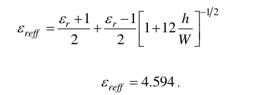
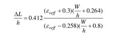
Various parameters required for designing the antenna is calculated using the following mathematical equations given below.
Given
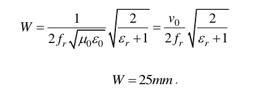

This design is optimized to the feed impedance for impedance matching and the ground plane dimensions were calculated as
Length of the ground plane = 25mm
Width of the ground plane = 9 mm.
B. Notch insertion
In order to improve the return loss and bandwidth of the antenna, additional notches were added. The following layout in Fig. 2.aillustrates an inverted L shaped notch inserted in the square patch on the left. The dimension of the horizontal portion of the notch is 8.3 mm and the vertical is 8.7 mm. The corresponding return loss characteristic is shown in Fig. 2.b, where resonances at 3.2 GHz, 5.3 GHz and 8.6 GHz are identified. A maximum return loss of -40dB occurring around 8.6 GHz frequency, is also observed.


(a) (b)
Fig. 2. (a) layout with one L notch (b) Return loss characteristics.
When another notch of length 11.6 mm, is inserted close to the L-shaped notch, the return loss at 8.6 GHz frequency is found to further reduce to – 47 dB. Fig. 3.a and b shows the layout and corresponding return loss behavior.


(a) (b)
Fig.3 (a) layout with two notches (b) Return loss characteristics
The third notch was inserted on a slot of patch on the right, in order to improve the return loss at 4 GHz. At this frequency, the return loss is nearly -10dB, which disrupts the wide band behaviour. The layout is depicted in Fig. 4.aFig. 4.a.


(a) (b)
Fig. 4. (a) layout with three notches (b) Return loss characteristics.
However, it is observed from the characteristics of three notch case (Fig. 4.b), a single notch was not effective enough to suppress the peak arising at 4GHz. Hence another notch of the same dimension is inserted near the third notch.
To calculate the notch dimension, the following expression is used 1111 Hany M. Zamel, Ahmed M.Attiya and Essam A. Hashish,” Design of compact UWB planar antenna with band notch characterisation.”, Proc. Radio Science conference,Cairo,2007,pp.18..
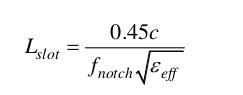
Be sure that the symbols in your equation have been defined before the equation appears or immediately following.
In the final design, the antenna has four notches in the patch out of which 3 of them are 11.6mm corresponding to a resonant frequency occurring at 5.4 GHz. Another notch is about 8.3 mm, inserted for 7.6 GHz frequency.
Fig. 5 illustrates the final antenna layout in ADS tool, which depicts the four notches clearly. The yellow color rectangle indicates the finite ground plane structure. The brown color layer with tapered edges above the ground plane indicates the radiating patch and the line below the ground plane is the microstrip line feed. The small extension visible below the feed line is the input port to the antenna.

Fig. 5. Final design layout in ADS tool.
The optimized design is then checked for momentum characteristics for measuring return loss and bandwidth parameters. The return loss characteristics depicted inFig. 6, reveals a better performance, without multiple peaks, which is a significant improvement over the previous report of Chen et al [8]. This results from the combined effect of finite ground plane and the multiple notches. The return loss charactersitics of various stages of development is illustrated in Fig. 7, which also incorporates the performance of previous design [8] for comparison. It is observed that the final design provides better return loss and required bandwidth.
The overall area of the antenna is calculated to be 25x25mm2.
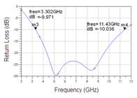
Fig. 6. Return loss characteristics obtained for the final layout.

Fig. 7. Return loss characteristics at different stages.
In order to examine the radiation performance of the antenna, current distributions are evaluated at different frequencies.

(a)
Fig. 8. Current distribution (a) 3.5 GHz
At 3.5GHz, the current vectors are primarily distributed near the feed region (Fig. 8.a), as the frequency increases the current at the feed region decreases gradually and tends to accumulate near the notch regions. At 8 GHz we observe that some part of the current is accumulated near the parallel notch region. This behavior is shown in Fig. 8.b and c.


(b) (c)
Fig. 8. Current distribution (b) 5 GHz (c) 8.6 GHz.

(a) (b)

(c) (d)
Fig. 9. (a) Electric field (b) Magnetic field (c) Gain pattern (d) Radiated power.
From the radiation pattern analysis, we observe that the antenna has a near isotropic radiation pattern, with a maximum efficiency of 54.7% at a frequency of 3.5GHz. The reduced efficiency is attributed to the FR-4 substrate. The electric field radiation, magnetic field, gain, radiated power and effective area obtained by ADS tool are shown in Fig. 9. The radiation pattern in 3-D view is shown in Fig. 10.

Fig. 10. 3D radiation pattern.
In the proposed design, a reasonable gain of 1.32dB has been obtained for a single patch and the return loss has been quite uniform without any peaks as in normal designs. The bandwidth measured at -10dB point shows that the antenna has a very large bandwidth of 8.28 GHz covering the entire UWB spectrum from 3.3GHz to 11.43GHz.
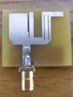
The designed antenna was fabricated with FR-4 substrate and is shown in Fig. 11. Also the test results obtained are compared with simulation plots to verify the design.

(a) (b)
Fig. 11. Fabricated antenna (a) Front view (b) Rear view.
This antenna is experimentally tested using a R&S ZVB 20GHz Vector Network Analyzer, for various parameters namely, return loss and voltage standing wave ratio (VSWR). The return loss characteristics are shown in Fig. 12, where the 10-dB bandwidth exceeds the required UWB range. However, the deviation from the simulation may be attributed to the fabrication, connector and soldering effects.
The voltage standing wave ratio varies between 1-1.5 in the frequency range of 3-12GHz in the test antenna and is shown in Fig. 13.
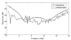
Fig. 12. Return loss.

Fig. 13. VSWR performance.
CONCLUSION
A simple design approach for UWB antenna is proposed. The base structure considered is investigated and additional design changes are incorporated to provide satisfactory results. We observe that the design results obtained is based on combined effects of the finite ground plane and multiple notches on the radiating patch on the FR-4 substrate. The fabricated antenna also provides a reasonable agreement with respect to the simulation results obtained. The antenna is found to provide a 10 dB bandwidth in excess of 8 GHz in the UWB band with a compact size of 25x25mm2. These antennas can be useful in small portable devices that require high bandwidth for large information carrying capacity at short distance.
acknowledgment
The authors would like to thank Mr.Ganesh Balasubramanian, Amphenol Omni Connect India Pvt. Ltd., for providing the measurement setup and Mrs.A.Kamalaveni, Research scholar for support throughout this work.
references
-
1Debmalya Bhattacharya, “Ultra Wide Band Microstrip Patch Antenna Design for Wireless Application.”, International Journal of Engineering Research And Technology (IJERT), Vol. 1 Issue 9, November-2012,pp.1-4.
-
2Jyoti R. Panda, Aditya S.R. Saladi and Rakhesh S. Kshetrimayum, “A Compact 3.4/5.5 GHz Dual Band-Notched UWB Monopole Antenna with Nested U-Shaped Slots.”, Proc. Second IEEE International conference on Computing, Communication and Networking Technologies, ICCNT 2010, pp.1-4.
-
3D.Punitharaj and S.Kalaimani, “Design and Fabrication of Microstrip Antenna for UWB Applications.”, International Journal of Emerging Trends in Electrical and Electronics, Vol. 3,No. 2, May-2013,pp.60 – 63.
-
4>Han Xiong, Jing-Song Hong, Yue-Hong Peng, “Impedance Bandwidth and Gain Improvement for Microstrip Antenna Using Metamaterials.”, Radio Engineering, Vol. 21, No. 4, December 2012,pp. 993- 998.
-
5M. Ojaroudi, Sh. Yazdanifard,N.Ojaroudi, and M. Naser-Moghaddasi, “Small Square Monopole Antenna With Enhanced Bandwidth by Using Inverted T-Shaped Slot and Conductor-Backed Plane.”, IEEE Trans. Antennas Propag., Vol. 59, No. 2, February 2011, pp. 670-674.
-
6Yashar Zehforoosh, Changiz Ghobadi and Javad Nourinia, “Antenna Design for Ultra Wideband Application Using a New Multilayer Structure.”, PIERS Online, Vol. 2, No. 6, 2006, pp. 544-549.
-
7L. Lolit Kumar Singh, Bhaskar Gupta and Partha.P.Sarkar, “A Review on effects of Finite Ground Plane on Microstrip Antenna Performance.”, International Journal of Electronics and Communication Engineering and Technology,Vol.3,No.3,2012,pp.287 -292.
-
8Zhi Ning Chen, Terence S. P. See, and Xianming Qing, “Small Printed Ultrawideband Antenna With Reduced Ground Plane Effect.”, IEEE Trans. Antennas Propag., Vol. 55, No.2,2007,pp. 383-388.
-
9Kyungho Chung, Jaemoung Kim and Jaehoon Choi, “Wideband Microstrip-Fed Monopole Antenna Having Frequency Band- Notch Function.”, IEEE Microw.Compon. Lett., Vol. 15, No.11,2005,pp.766-768.
-
10Nasser Ojaroudi and Mohammad Ojaroudi, “Novel Design of Dual Band-Notched Monopole Antenna With Bandwidth Enhancement for UWB Applications.”, IEEE Antennas Wireless Propag. Lett., Vol. 12, 2013 pp. 698-701.
-
11Hany M. Zamel, Ahmed M.Attiya and Essam A. Hashish,” Design of compact UWB planar antenna with band notch characterisation.”, Proc. Radio Science conference,Cairo,2007,pp.18.
Publication Dates
-
Publication in this collection
June 2015
History
-
Received
05 Nov 2014 -
Reviewed
06 Nov 2014 -
Accepted
16 Apr 2015


