Abstract
In this paper, a finite-difference time-domain (FDTD) formulation, based on the exponential matrix and on thin material sheet methods is developed for modeling subcellular thin graphene sheets. This formulation is validated by reproducing graphene frequency selective surfaces (FSS) known from literature. Then, we propose in this work a smart graphene FSS device. Smartness is obtained by means of a unity cell formed by a graphene ring with a graphene sheet placed in its aperture. By properly regulating the chemical potentials of the graphene elements, two frequency- tunable modus operandi are obtained: single- or dual-band rejection modes. When the device operates in its dual-band rejection mode, either of the rejection bands can be shifted individually in the frequency spectrum. Additionally, both rejection bands can also be reconfigured simultaneously.
Index Terms
FDTD Method; Graphene; Matrix Exponential Method; Smart FSS
I. INTRODUCTION
Frequency selective surfaces (FSS) are structures used as filters [11 [1] M. Bashiri, C. Ghobadi, J. Nourinia, and M. Majidzadeh, “WiMAX, WLAN, and X-Band Filtering Mechanism: Simple-Structured Triple-Band Frequency Selective Surface,” IEEE Antennas and Wireless Propagation Letters, vol. 16, pp. 3245-3248, Nov. 2017.], which are employed usually by periodically distributing optimized unit cells over surfaces. FSSs have a great number of applications in telecommunications, such as in designing of radomes, absorbers and electromagnetic shielding structures [11 [1] M. Bashiri, C. Ghobadi, J. Nourinia, and M. Majidzadeh, “WiMAX, WLAN, and X-Band Filtering Mechanism: Simple-Structured Triple-Band Frequency Selective Surface,” IEEE Antennas and Wireless Propagation Letters, vol. 16, pp. 3245-3248, Nov. 2017.]. In this context, FSSs operate as band-reject filters, of which rejection band(s) is(are) dependent on the geometry (unit cell configuration) and materials of their constitutive elements. Additionally, thickness and material parameters of substrate are also important design parameters [22 [2] E. S. Torabi, A. Fallahi, and A. Yahaghi, “Evolutionary Optimization of Graphene-Metal Metasurfaces for Tunable Broadband Terahertz Absorption,” IEEE Transactions on Antennas and Propagation, vol. 65, no. 3, pp. 1464-1467, Mar. 2017.]. However, traditional (metallic) FSSs do not have dynamic adjustment of central frequencies of their rejection bands. In order to obtain such functionality, graphene has been incorporated into recently proposed FSS designs [33 [3] M. Qu et al., “Design of a Graphene-Based Tunable Frequency Selective Surface and Its Application for Variable Radiation Pattern of a Dipole at Terahertz,” Radio Science, vol. 53, no. 2, pp. 183-189, Jan. 2018.].
Graphene is a two-dimensional material consisting of a planar arrangement of carbon atoms, of which electrical properties are of particular interest [44 [4] K. S. Novoselov and A. K. Geim, “The Rise of Graphene,” Nat. Mater., vol. 6, no. 3, pp. 183-191, Mar. 2007.], such as the dynamic control of the complex surface conductivity by regulating chemical potential μc, as described by Kubo formalism [55 [5] G. W. Hanson, “Dyadic Green's functions and guided surface waves for a surface conductivity model of graphene,” J. Appl. Phys., vol.103, no. 6, p. 064302, Mar. 2008.]. Tuning of μc is performed by means of a controlled external transverse DC electric field, which in turn is controlled by a gate voltage VDC applied between the graphene sheet and an electrode. According to [66 [6] J. S. Gómez-Díaz and J. Perruisseau-Carrier, “Graphene-based plasmonic switches at near infrared frequencies,” Optics Express, vol. 21, no. 13, pp. 15490-15504, 2013.], , where ћ is the reduced Plank constant, vf is the Fermi velocity, ε is the electric permittivity between the voltage source terminals, e is the electron charge and Ge is the gate extent. Typically, 0 ≤ |μc| ≤ 1 eV and 0 ≤ |VDC| ≤ 1000 V.
Hybrid FSSs designed with graphene and metallic parts have been proposed [77 [7] M. Qu, M. Rao, S. Li, and L. Deng, “Tunable antenna radome based on graphene frequency selective surface,” AIP Advances, vol. 7, no. 9, p. 095307, 2017.]-[99 [9] D. W. Wang et al., “Tunable THz Multiband Frequency-Selective Surface Based on Hybrid Metal-Graphene Structures,” IEEE Transactions on Nanotechnology, vol. 16, no. 6, pp. 1132-1137, Nov. 2017.], providing reconfigurable rejection band. The electrical conductivity of graphene can also be modified by applying external magnetic field, increasing the degrees of freedom to dynamically reconfigure FSSs [1010 [10] L. Lin, L. S. Wu, W. Y. Yin, and J. F. Mao, “Modeling of magnetically biased graphene patch frequency selective surface (FSS),” in 2015 IEEE MTT-S International Microwave Workshop Series on Advanced Materials and Processes for RF and THz Applications (IMWS-AMP), Jul. 2015, pp. 1-3.], [1111 [11] P. K. Khoozani, M. Maddahali, M. Shahabadi, and A. Bakhtafrouz, “Analysis of magnetically biased graphene-based periodic structures using a transmission-line formulation,” J. Opt. Soc. Am. B, vol. 33, no. 12, pp. 2566-2576, Dec. 2016.].
In this work, a smart FSS composed only of graphene elements and a glass substrate is proposed. The main contribution of this paper consists on a novel class of smart reconfigurability, which is obtained by optimizing the proposed unity cell designed with a graphene ring and a graphene sheet placed in its aperture. By adjusting the chemical potentials of two graphene elements of the unit cell, the novel FSS device can operate as: a) reconfigurable single-band filter or b) reconfigurable dualband filter. When the proposed FSS operates in its single-band mode, smartness provides dynamical frequency reconfiguration of the rejection band. On the other hand, when the proposed FSS operates in its dual-band mode, smartness provides the following capabilities: b.1) dynamical frequency reconfiguration of either of the rejection bands individually, i.e., maintaining the other one fixed, b.2) dynamical frequency offset of both rejection bands simultaneously. It is important to notice that the ability to operate as single or dual band device is not among the capabilities of graphene FSSs designed in previously published papers such as [22 [2] E. S. Torabi, A. Fallahi, and A. Yahaghi, “Evolutionary Optimization of Graphene-Metal Metasurfaces for Tunable Broadband Terahertz Absorption,” IEEE Transactions on Antennas and Propagation, vol. 65, no. 3, pp. 1464-1467, Mar. 2017.], [33 [3] M. Qu et al., “Design of a Graphene-Based Tunable Frequency Selective Surface and Its Application for Variable Radiation Pattern of a Dipole at Terahertz,” Radio Science, vol. 53, no. 2, pp. 183-189, Jan. 2018.] and [1010 [10] L. Lin, L. S. Wu, W. Y. Yin, and J. F. Mao, “Modeling of magnetically biased graphene patch frequency selective surface (FSS),” in 2015 IEEE MTT-S International Microwave Workshop Series on Advanced Materials and Processes for RF and THz Applications (IMWS-AMP), Jul. 2015, pp. 1-3.]. Recently, Tasolamprou et al. conducted experiments in [1212 [12] A. C. Tasolamprou, A. D. Koulouklidis, C. Daskalaki, C. P. Mavidis, G. Kenanakis, G. Deligeorgis, Z. Viskadourakis, P. Kuzhir, S. Tzortzakis, M. Kafesaki, E. N. Economou and C. M. Soukoulis, “Experimental demonstration of ultrafast THz modulation in a graphene-based thin film absorber through negative photoinduced conductivity,” ACS photonics, vol. 6, no. 3, pp. 720-727, 2019.] regarding measurements of THz waves interacting with graphene sheet set up over an SU-8 substrate, showing real feasibility of fabricating the device proposed in this paper.
In addition, an improved FDTD formulation, mainly based on Matrix Exponential technique [1313 [13] X. H. Wang, W. Y. Yin, and Z. Chen, “Matrix Exponential FDTD Modeling of Magnetized Graphene Sheet,” IEEE Antennas and Wireless Propagation Letters, vol. 12, pp. 1129-1132, 2013.], is developed for calculating electric field and electric current density vectors on graphene sheets. It is demonstrated that the formulation produces a subcellular thin sheet of which thickness is that of graphene. The proposed formulation and smart FSS are validated by performing comparisons of FDTD solutions with those of commercial software such as HFSS [1414 [14] ANSYS. HFSS. [Online]. Available: ansys.com/products/electronics.
ansys.com/products/electronics...
], COMSOL and CST.
II. MATHEMATICAL FORMULATION
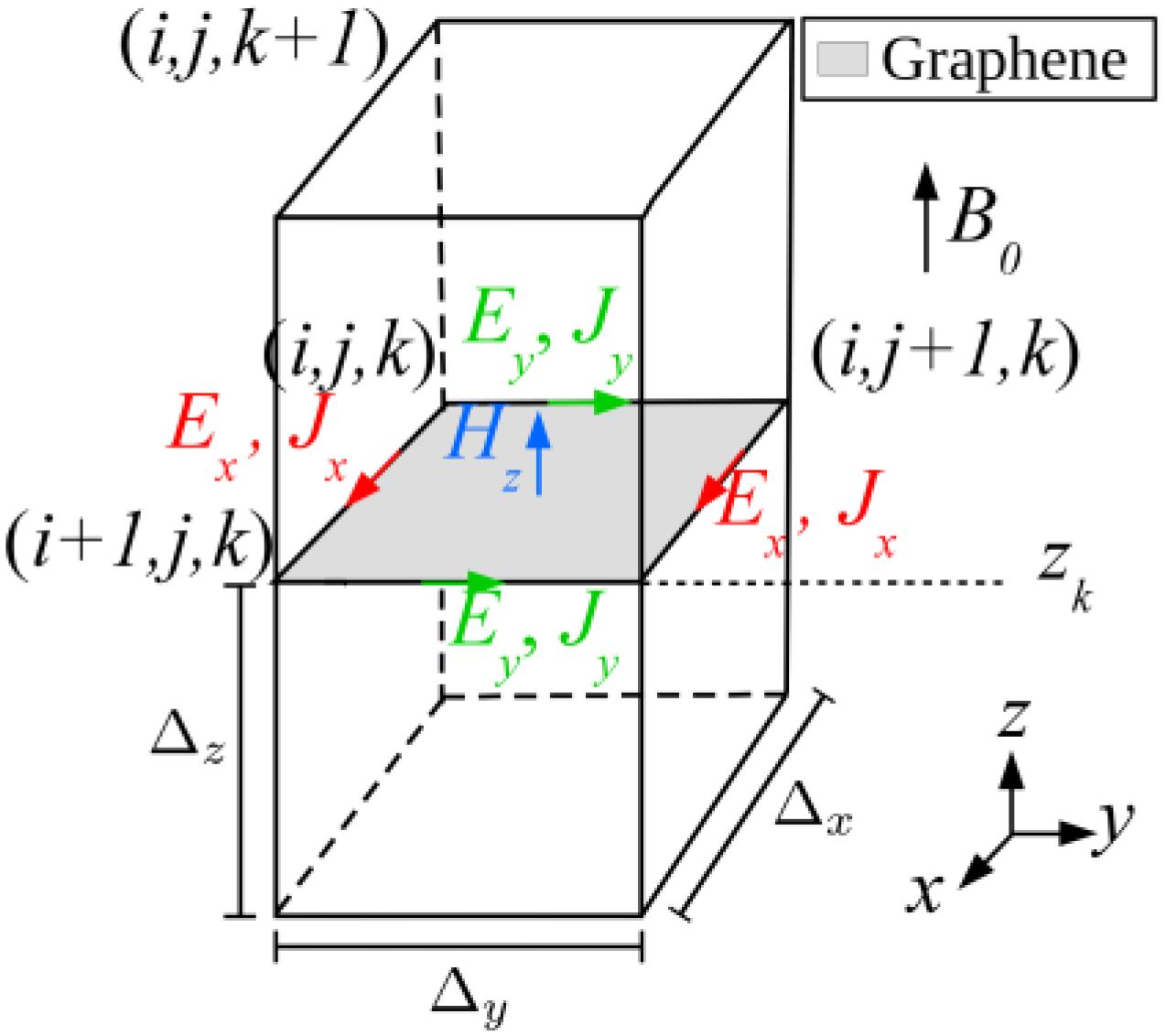
In FDTD lattices, graphene sheets can be modeled as subcellular planar objects, similarly to the formulation developed in [1515 [15] R. M. S. de Oliveira, N. R. N. M. Rodrigues and V. Dmitriev, “FDTD Formulation for Graphene Modeling Based on Piecewise Linear Recursive Convolution and Thin Material Sheets Techniques,” IEEE Antennas and Wireless Propagation Letters, vol. 14, pp. 767-770, 2015.]. Yee cell faces containing electric field components defining TE modes are used for performing the subcellular representation of graphene, such as illustrated by Fig. 1 for the TEz mode [1313 [13] X. H. Wang, W. Y. Yin, and Z. Chen, “Matrix Exponential FDTD Modeling of Magnetized Graphene Sheet,” IEEE Antennas and Wireless Propagation Letters, vol. 12, pp. 1129-1132, 2013.], [1515 [15] R. M. S. de Oliveira, N. R. N. M. Rodrigues and V. Dmitriev, “FDTD Formulation for Graphene Modeling Based on Piecewise Linear Recursive Convolution and Thin Material Sheets Techniques,” IEEE Antennas and Wireless Propagation Letters, vol. 14, pp. 767-770, 2015.].
Subcellular FDTD modeling of graphene sheet in the Yee cell (i,j,k) based on specific updating equations for tangential components of and under influence of .
The numerical representation of graphene is based on specific updating equations used to calculate the components of electric field and current density which are tangential to the sheet [1313 [13] X. H. Wang, W. Y. Yin, and Z. Chen, “Matrix Exponential FDTD Modeling of Magnetized Graphene Sheet,” IEEE Antennas and Wireless Propagation Letters, vol. 12, pp. 1129-1132, 2013.] (Ex, Ey, Jx and Jy in Fig. 1). The influence of normal component of external magnetic flux density can be considered.
According to the Drude model, disregarding interband contributions, the conductivity of the graphene can be represented by the tensor [1313 [13] X. H. Wang, W. Y. Yin, and Z. Chen, “Matrix Exponential FDTD Modeling of Magnetized Graphene Sheet,” IEEE Antennas and Wireless Propagation Letters, vol. 12, pp. 1129-1132, 2013.] [1616 [16] D. L. Sounas and C. Caloz, “Gyrotropy and Nonreciprocity of Graphene for Microwave Applications,” IEEE Transactions on Microwave Theory and Techniques, vol. 60, no. 4, Apr. 2012.]
where
and
In (2) and (3), is the cyclotron frequency, B0 is the normal component of external magnetic flux density and vF is the Fermi velocity. In (4), qe is the electron charge, kB is the Boltzmann constant, T is the temperature, ћ is the reduced Planck's constant, τ is the transport relaxation time and μc is the chemical potential of graphene [55 [5] G. W. Hanson, “Dyadic Green's functions and guided surface waves for a surface conductivity model of graphene,” J. Appl. Phys., vol.103, no. 6, p. 064302, Mar. 2008.].
Fig. 2 shows the conductivity (real and imaginary parts) and λSPP (plasmon wavelength [1717 [17] P. Gonçalves and N. Peres, An Introduction to Graphene Plasmonic. World Scientific, 2016, ch. 3, pp 47-66.] for infinite area graphene sheet), as a function of the chemical potential μc, considering the isotropic model of graphene (B0 = 0). As shown in Fig. 2, as μc increases gradually, the real part of the conductivity and λSPP increase, and so it does . The gradual increase of the absolute conductivity, as inferred from Figs. 2(a) and 2(b), is related to a higher level of electromagnetic wave reflection incident on surfaces composed of graphene. As for λSPP, the increase caused by the gradual change of μc has a direct influence on the increase in plasmon wave velocity vG, since
and
for when B0 = 0, where kSPP is the plasmon wavenumber and f is the frequency. The parameters k0 and η0 are the well-known free space wavenumber and wave impedance, respectively.
The real part of the conductivity of graphene is illustrated in (a), its imaginary part in (b) and λSPP in (c), for B = 0 T, as functions of the chemical potential μc.
On the region containing the graphene sheet, the frequency domain Ampère's law can be written as
where , and are the Fourier transforms of the electric field, magnetic field and electric current volumetric density, respectively. Provided that the thin graphene sheet of interest is positioned at z = zk, such as illustrated by Fig. 1, its surface conductivity can be described in terms of the Dirac impulse function [1818 [18] Ž. i. Kancleris, G. Slekas, and A. Matulis, “Modeling of Two-Dimensional Electron Gas Sheet in FDTD Method,” IEEE Transactions on Antennas and Propagation, vol. 61, no. 2, pp. 994–996, Feb. 2013.] by
Integrating (7) in the interval [zk – Δz / 2, zk + Δz / 2], where Δz is the length of the Yee cell edge parallel to z (Fig. 1), and applying the sampling property of the impulse function, one obtains
in which is the surface current density. By using (1) and (8), one has
Thus, we may write
and
Applying (2) and (3) to (10), using (11) and transforming (10) to time domain produce
Similar mathematical procedures executed applying (2) and (3) to (11) and using (10) yield
Equations (12) and (13) can be written using a compact matrix notation as
in which
In (15), Γ = 1/ (2τ) is the scattering rate.
In order to solve the matrix differential equation given in (14), the matrix exponential method is applied [1313 [13] X. H. Wang, W. Y. Yin, and Z. Chen, “Matrix Exponential FDTD Modeling of Magnetized Graphene Sheet,” IEEE Antennas and Wireless Propagation Letters, vol. 12, pp. 1129-1132, 2013.], [1919 [19] D. Y. Heh and E. L. Tan, “FDTD Modeling for Dispersive Media Using Matrix Exponential Method,” IEEE Microwave and Wireless Components Letters, vol. 19, no. 2, pp. 53–55, Feb. 2009.]. At first, (14) is transformed to Laplace domain. Subsequently, after performing the proper mathematical manipulations, one sees that
Then, by applying the inverse Laplace transform in (16), we have
In the FDTD method, and are calculated, in the discrete time lattice, at instants (η + ½) Δt and nΔt, respectively [2020 [20] A. Taflove and S. C. Hagness, “Introduction to Maxwell’s Equations and the Yee algorithm, Incident Wave Source Conditions,” in Computational Electrodynamics: The Finite-Difference Time-Domain Method. Norwood, MA, USA: Artech House, 2005, ch. 3,5, pp. 58–79,186–201.]. Consequently,
where
and
Equations (19) and (20) can be simplified using the matrix exponential method. Therefore, both equations are written in terms of the eigenvalues of M as
and
in which
and
Therefore, the discrete equations for updating Jx and Jy are given by
and
Differently from what is proposed in [1313 [13] X. H. Wang, W. Y. Yin, and Z. Chen, “Matrix Exponential FDTD Modeling of Magnetized Graphene Sheet,” IEEE Antennas and Wireless Propagation Letters, vol. 12, pp. 1129-1132, 2013.], in this work components of surface current density tangential to graphene sheets are calculated at the same spatial positions defined by Yee for calculating the corresponding components of electric field, such as Fig. 1 illustrates for a graphene sheet placed parallelly to the x-y plane. This is necessary for performing physically-appropriate calculations of the components of and on graphene sheets. This is due to the interdependence between Jx and Jy, specified by (12) and (13), which follows from the tensor nature of the electrical conductivity (1). In this way, spatial averages of the field components must be considered for computing (25) and (26). Therefore, we have
and
Similar procedure is carried out for the field components and .
Once the scalar components of have been calculated on the graphene sheet, time domain Ampère's Law must be used for computing components of . Thus, the FDTD equation for updating Ex is
In an analogous way, it is possible to obtain a FDTD equation for . Notice that dividing Jx by Δz in (29), as required by (8), produces an effective conductivity on the sheet proportional to the volume occupied by the graphene sheet in the Yee cell, according to the FDTD thin material sheet technique [2121 [21] J. Maloney and G. Smith, “The efficient modeling of thin material sheets in the finite-difference time-domain (FDTD) method,” IEEE Transactions on Antennas and Propagation, vol. 40, no. 3, pp. 323–330, Mar 1992.], which has been directly employed in [1515 [15] R. M. S. de Oliveira, N. R. N. M. Rodrigues and V. Dmitriev, “FDTD Formulation for Graphene Modeling Based on Piecewise Linear Recursive Convolution and Thin Material Sheets Techniques,” IEEE Antennas and Wireless Propagation Letters, vol. 14, pp. 767-770, 2015.] for modeling graphene. In short, physical surface conductivity of graphene is given by , in which d is the real thickness of the graphene sheet [55 [5] G. W. Hanson, “Dyadic Green's functions and guided surface waves for a surface conductivity model of graphene,” J. Appl. Phys., vol.103, no. 6, p. 064302, Mar. 2008.], Thus, as previously stated, . Therefore, , justifying the choice of the integration interval used to produce (8). Finally, Ez and all components of are calculated exactly as in the original FDTD method [20], In this work, the programming language C was employed for implementing the proposed method.
III. VALIDATION OF THE DEVELOPED FORMULATION
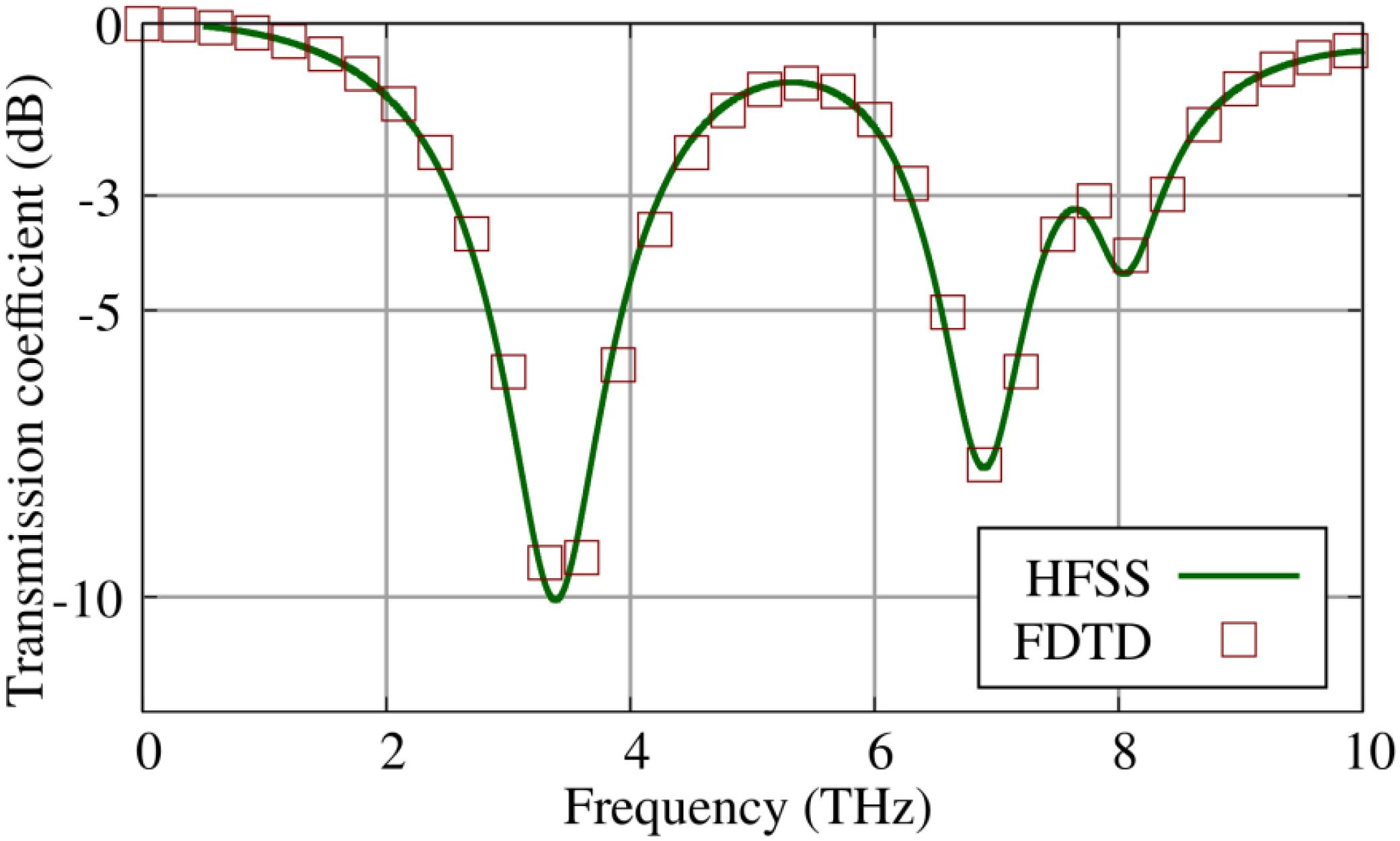
In order to validate the FDTD formulation presented in Section II, the frequency response of the graphene FSS described in [1010 [10] L. Lin, L. S. Wu, W. Y. Yin, and J. F. Mao, “Modeling of magnetically biased graphene patch frequency selective surface (FSS),” in 2015 IEEE MTT-S International Microwave Workshop Series on Advanced Materials and Processes for RF and THz Applications (IMWS-AMP), Jul. 2015, pp. 1-3.] is reproduced in this paper. The numerical solutions obtained using the FDTD routine developed in this work are compared with results calculated employing HFSS.
The FSS modeled for validation purposes is illustrated by Fig. 3. The square unit cells have sides (period) measuring D = 5 μm. The edge length of each square graphene element of the periodic structure is D – g, where g = 0.5 μm. The parameters of the FSS graphene sheets are μc = 0.5 eV, τ = 0.5 ps and T = 300 K. For proper comparison of results with those provided by [1010 [10] L. Lin, L. S. Wu, W. Y. Yin, and J. F. Mao, “Modeling of magnetically biased graphene patch frequency selective surface (FSS),” in 2015 IEEE MTT-S International Microwave Workshop Series on Advanced Materials and Processes for RF and THz Applications (IMWS-AMP), Jul. 2015, pp. 1-3.], the graphene structure is simulated in free space (i.e., the substrate relative permittivity is εr = 1 and h is consequently irrelevant for this case). Finally, the structure is under influence of external magnetostatic field , in which B0 = 1 T.
Geometry of the FSS of [1010 [10] L. Lin, L. S. Wu, W. Y. Yin, and J. F. Mao, “Modeling of magnetically biased graphene patch frequency selective surface (FSS),” in 2015 IEEE MTT-S International Microwave Workshop Series on Advanced Materials and Processes for RF and THz Applications (IMWS-AMP), Jul. 2015, pp. 1-3.] (perspective view of part of the periodic structure).
The computational domain used in the FDTD method to represent the unit cell of the FSS under analysis has 20×20×400 cells. In this mesh, the Yee cells are cubic, with edges measuring Δ = 0.25 μm. Beneath and above the periodic structure, convolutional perfectly matched layer (CPML) formulation [2222 [22] J. A. Roden and S. D. Gedney, “Convolution PML (CPML): An efficient FDTD implementation of the CFS-PML for arbitrary media,” Microwave and Optical Tech. Letters, vol. 27, no. 5, pp. 334–339, 2000.] is used, absorbing electromagnetic waves propagating outwardly the FDTD lattice. Periodicity is achieved by applying the PBC (Periodic Boundary Condition) technique defined in [2323 [23] F. Yang, J. Chen, R. Qiang, and A. Elsherbeni, “A simple and efficient FDTD/PBC algorithm for scattering analysis of periodic structures,” Radio Science, vol. 42, no. 4, pp. 1–9, Aug. 2007.] at the side ends of a single period of the FSS. The FSS is excited by a x-polarized plane wave generated using the TF/SF technique (Total-Field/Scattered-Field) [2020 [20] A. Taflove and S. C. Hagness, “Introduction to Maxwell’s Equations and the Yee algorithm, Incident Wave Source Conditions,” in Computational Electrodynamics: The Finite-Difference Time-Domain Method. Norwood, MA, USA: Artech House, 2005, ch. 3,5, pp. 58–79,186–201.], of which temporal profile is governed by a Gaussian pulse with a minimum significant spectral amplitude at f = 20 THz.
In HFSS, graphene sheets are modeled as anisotropic surface impedances (designation of the boundary condition in that software). Real and imaginary parts of each element of σ−1(ω) (denoted by Zs(ω) in the HFSS) over the entire frequency range under analysis are imported using an auxiliary file. The matrix σ−1(ω) is the inverse of (1). The excitation element called Floquet port and the Master and Slave boundary conditions are used to enforce the periodicity to the problem.
Fig. 4 shows the co-polarization transmission coefficient obtained in this work using the proposed FDTD modeling of graphene and HFSS. Over the full band of interest (0.5 – 10 THz), the frequency responses obtained using FDTD and HFSS show good agreement with results presented in [1010 [10] L. Lin, L. S. Wu, W. Y. Yin, and J. F. Mao, “Modeling of magnetically biased graphene patch frequency selective surface (FSS),” in 2015 IEEE MTT-S International Microwave Workshop Series on Advanced Materials and Processes for RF and THz Applications (IMWS-AMP), Jul. 2015, pp. 1-3.], in which the minimum co-polarization transmission coefficient is 0.22 for the structure of Fig. 3, occurring approximately at 4.70 THz.
IV. THE PROPOSED SMART FSS: DESIGN, ANALYSIS AND RESULTS
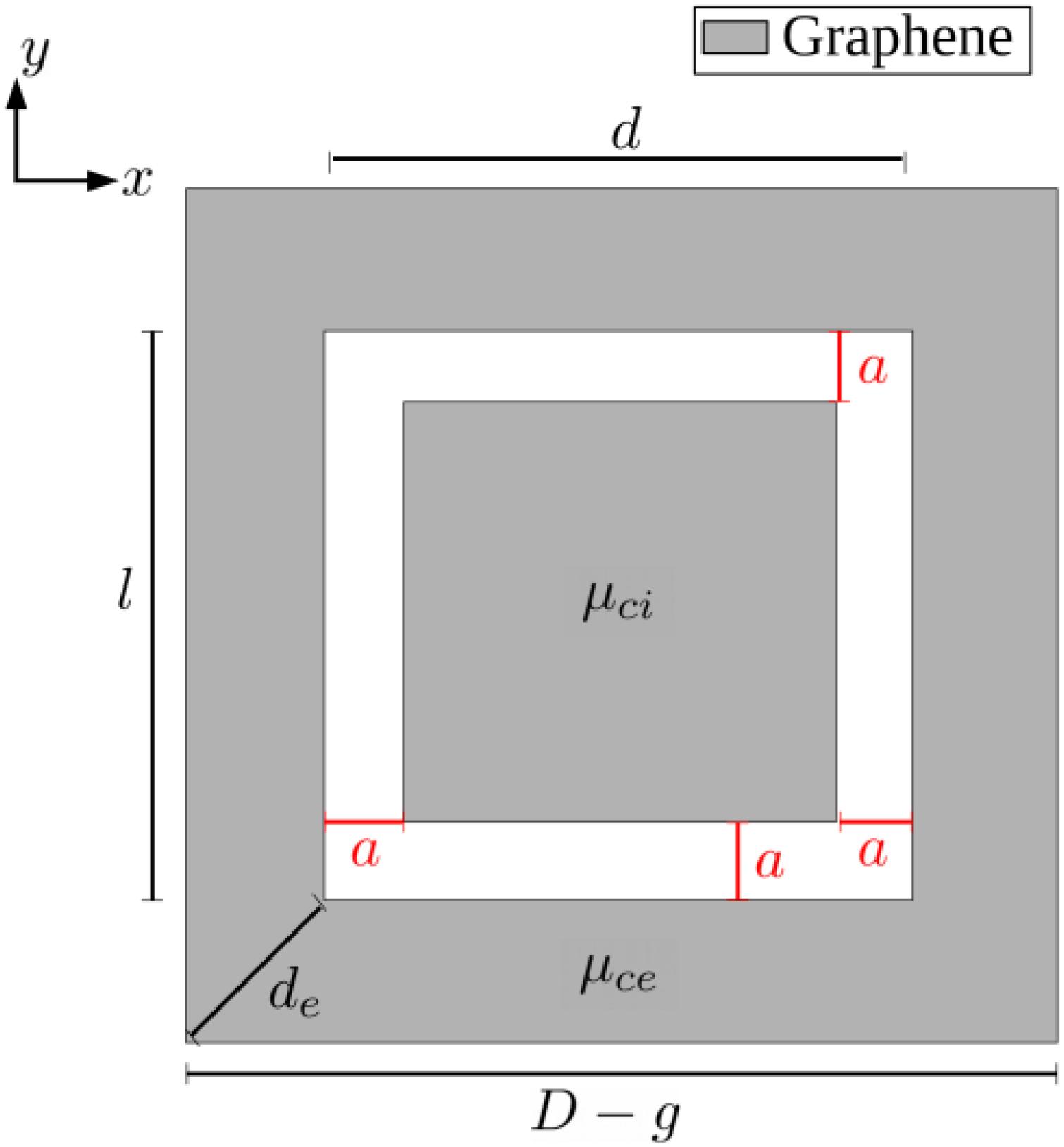
In this section, a smart graphene FSS is proposed. The unit cell of the structure of Fig. 3 is replaced by the unit cell illustrated by Fig. 5. It is composed of two graphene elements: a square ring with chemical potential μce and a graphene sheet placed coplanarly to the ring, in its aperture, with chemical potential μci. The proposed FSS has the following fixed parameters: D = 5 μm, g = 0.5 μm and a = 100 nm. In addition, the magnetostatic field is not applied to the structure (B0 = 0). Notice that those fixed parameters are based on the FSS proposed in [1111 [11] P. K. Khoozani, M. Maddahali, M. Shahabadi, and A. Bakhtafrouz, “Analysis of magnetically biased graphene-based periodic structures using a transmission-line formulation,” J. Opt. Soc. Am. B, vol. 33, no. 12, pp. 2566-2576, Dec. 2016.], of which unit cell has solely the square graphene ring with aperture edges measuring d = l = 2.25 μm (lacking the internal graphene sheet proposed in this work). Every graphene element of the unit cell is set up with τ = 0.25 ps and T = 300 K. The substrate is characterized by the parameters εr = 3.9 and h = 1 μm.
The unit cell of the FSS proposed in this work for dynamic change of the state of operation and smart tuning of rejection band(s).
A. Design of a smart graphene FSS operating as dual-band or single band filter
As a preliminary procedure to obtain the smart multiband FSS, we analyze the spectral response of an FSS of which unit cell is formed by a graphene ring set up with μce = 1 eV and a rectangular aperture with the geometric parameters d = 0.25 μm, l = 2.25 μm and de = 1.59μm, as indicated in Fig. 5. For this initial analysis, the graphene sheet in the ring aperture is not included in the unit cell. This configuration is investigated via FDTD and HFSS to demonstrate that a rectangular opening in the graphene ring used as the FSS unit cell produces more than one rejection band. This analysis is a first step towards the design of the proposed smart FSS device. In FDTD simulations, the uniform computational mesh has 160×160×400 cubic Yee cells, of which edges measure 31.25 nm.
As it can be seen in results of Fig. 6, this periodic structure has two rejection bands (i.e., it is a dual-band FSS). By considering the rejection level of −4 dB as reference, the lower-band rejection window has relative bandwidth of 40 %, ranging from 2.70 THz to 4.05 THz. In this frequency range, the minimum transmission of −10.05 dB is seen at the frequency of 3.39 THz. The bandwidth of the higher-frequency rejection band (6.43 – 7.38 THz) is 13.76%. The minimum transmission is −7.71 dB at 6.93 THz.
Comparison between FDTD and HFSS results: FSS co-polarization transmission coefficient for the graphene ring with rectangular aperture with dimensions d = 0.25 μm and l = 2.25 μm, without the internal graphene sheet. For the graphene ring, μce is set to 1 eV.
Fig. 7(a) shows the spatial distribution of surface current density for a FSS with unit cell formed by the square graphene ring (no graphene sheet in its aperture) at its resonance frequency of 3.29 THz. On the other hand, Fig. 7(b) shows distribution obtained when a graphene sheet is placed in its aperture. For the case of Fig. 7(b), the chemical potential μci is set to the negligible value of 1 meV, making it more transparent than the ring, which is configured with μce = 0.75 eV. Due to the small conductivity level on the graphene sheet (see Fig. 2), its current density level is considerable smaller than that seen on the ring. As it can be seen by comparing Figs. 7(a) and 7(b), the obtained current distributions on the rings are extremely similar, characterizing the same type of resonance.
(A/m2) for the following FSSs: (a) square ring only, μce = 1 eV and d = l = 2.25 μm at f = 3.29 THz and (b) square ring with the graphene sheet in its aperture, μce = 0.75 eV, μci = 1 meV and a = 100 nm, for f = 2.65 THz (first resonance).
Figs. 8(a) and 8(b) show distributions of obtained for the FSS based on the rectangular aperture graphene ring (of which transmission coefficients are shown by Fig. 6) at frequencies of minimum transmission in each rejection band (3.39 THz and 6.93 THz). In Fig. 8(a), obtained at the first resonance of the device, it is shown the establishment of a dipole mode, similarly to that seen in Fig. 7(a) for the case of the square aperture ring. In contrast, Fig. 8(b) shows a quadrupole mode for the second resonance of the structure, which is a clear consequence of the fact that d ≠ i. For the cases of Fig. 7, the single resonance frequency observed in the analyzed spectral range for the square ring is caused mainly by the intense currents flowing from one of the outer borders of the ring, parallel to y, to the border on the opposite side, separated by the distance D – g (see Fig. 5). This is also observed in Fig. 8(a) for the first resonance of the rectangular aperture ring. However, the second resonance of FSS based on the rectangular aperture ring is driven mainly by the intense currents flowing between edges of the ring and edges of the rectangular aperture (which are set apart by the distance (D – g – d)½, as it is perceptible by inspecting Fig. 8(b). This justifies the fact that the second resonance frequency (6.93 THz) is higher than twice the first resonance frequency (3.39 THz).
for the FSSs configured with μce = 1 eV and with the following parameters: (a) d = 0.25 μm and l = 2.25 μm for f = 3.39 THz (first resonance, with no graphene sheet in the ring aperture), (b) d = 0.25 μm and l = 2.25 μm for f = 6.93 THz (second resonance, with no graphene sheet in the ring aperture) (c) μci = 1 eV and a = 100 nm, for f = 2.78 THz (first resonance of the proposed FSS), (d) μci = 1 eV and a = 100 nm, for f = 6.21 THz (second resonance of the proposed FSS).
Thus, the main idea grounding the design of the proposed smart FSS is using the graphene sheet at the rectangular aperture of the ring to turn on or off the high-frequency rejection band, producing two reconfigurable operation modes. This is possible because setting the chemical potential of a graphene sheet to zero makes it practically transparent for electromagnetic waves and the increment of this parameter increases electrical conductivity of the graphene element (see Fig. 2). For the cases in which μci = 0 and μce ≅ 1, the FSS operates mainly due the intense currents seen on the ring of Fig. 8(c) (dipole mode), which is similar to the current distribution seen in Fig. 7(a) for the case based on the ring only. Additionally, when μci approaches 1eV, a second resonance is created, working supported not only by the current distribution on the ring seen in Fig. 8(d), which is similar to the quadrupole mode of Fig. 8(b) of the rectangular aperture ring second resonance. It is also supported by the currents induced on the graphene sheet in the ring aperture. In summary, when μce and μci are much larger than zero simultaneously, the space a between the ring and the internal graphene sheet works similarly to the rectangular aperture of Fig. 8(b). Further, when μci approaches zero, the inner sheet becomes nearly transparent and the FSS behaves analogously as the structure of Fig. 7(a).
For the proposed smart FSS, the dimensions associated to the aperture are d = l = 2.25 μm, and the distance between the border of the aperture and the graphene sheet is a = 100 nm. In the FDTD method, a uniform computational mesh with 200×200×400 cubic Yee cells is used (Δx = Δy = Δz = 25 nm). In the mesh created using HFSS, the minimum and maximum edges of the triangular elements are 13 nm and 270 nm, respectively. This finite element mesh is shown in Fig. 9.
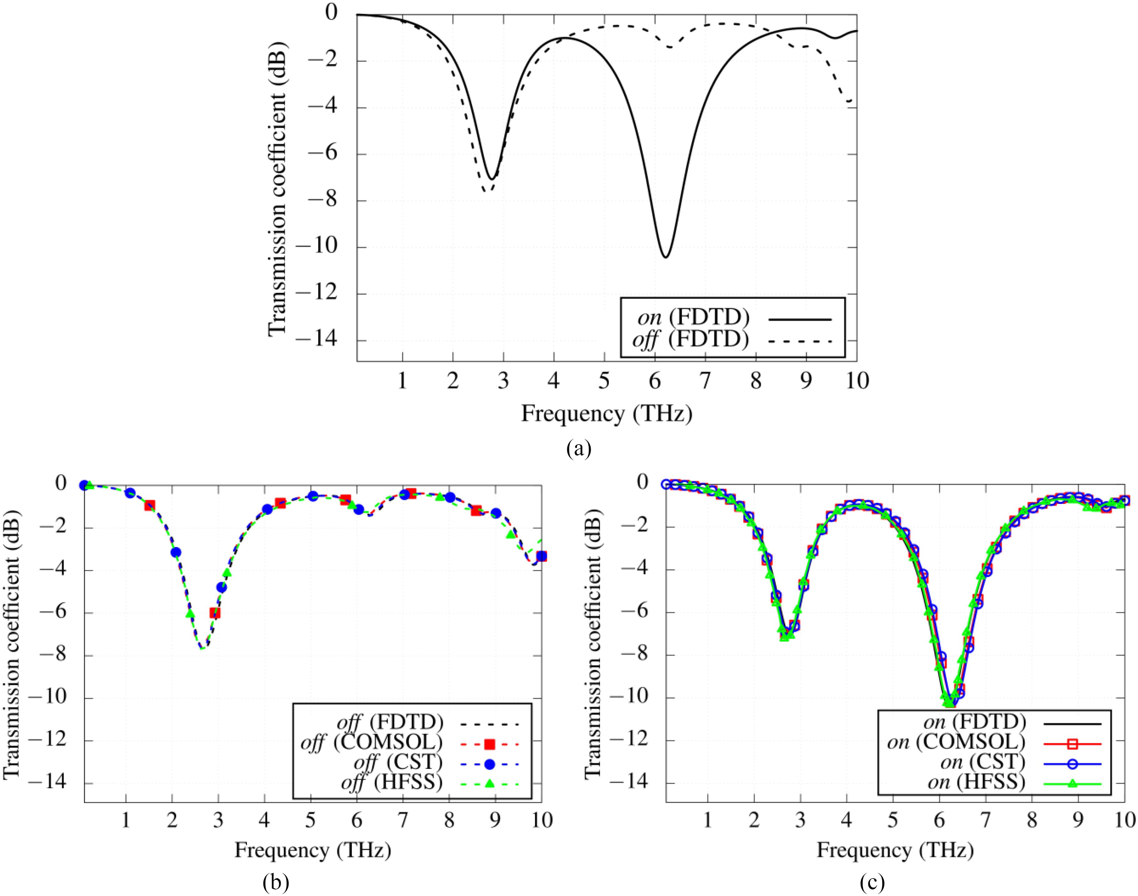
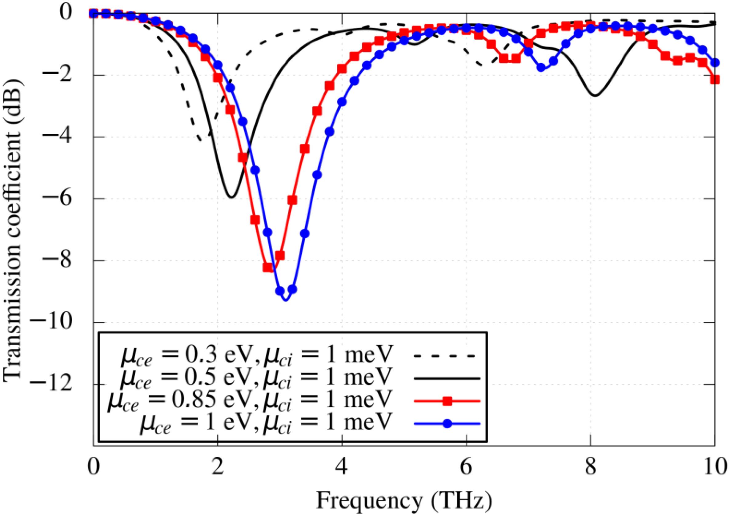
The first operation state is the dual-band mode (mode on). As previously explained, it can be obtained by, for example, setting μce = μci = 1 eV. For this state setup, the first rejection band has a relative bandwidth of 29.30 % (2.36 – 3.17 THz), where the minimum transmission is −7.19 dB at 2.78 THz. The second transmission rejection band has a bandwidth of 23.30 % (5.50 – 6.95 THz), of which transmission minimum is −10.27 dB at f = 6.21 THz. As Fig. 10 shows, the transmission minimum in the higher-band rejection window is 3 dB lower than the minimum of the first rejection band. This is expected since the lower-frequency rejection band is mainly supported by the currents induced on the ring and the high-frequency rejection band is supported not only by induced currents on the graphene ring, but also by induction on the graphene sheet in the ring aperture. This physical behavior can be appreciated by inspecting Figs. 8(c) and 8(d), which illustrate for the frequencies corresponding to the first and the second transmission minima, respectively.
Co-polarization transmission coefficient for a = 100 nm: (a) the two proposed FSS operation configurations, (b) validation of FDTD model for the off mode and (c) validation of FDTD model for the on mode.
The second operation state is single-band mode (mode off), which can be obtained by fixing μce = 0.75 eV and μci = 1 meV. In this state, the device works with a single frequency band of low transmission levels since the graphene sheet placed in the square-aperture ring is virtually transparent. The parameter μce is set to 0.75 eV in order to maximize the coincidence of the single spectral rejection range to the lower resonance band of the dual-band mode. Thus, the minimum transmission is −7.66 dB at f = 2.65 THz. The relative bandwidth in this single-mode configuration is approximately 37.50% (2.21 – 3.23 THz), slightly smaller than the bandwidth of the lower resonance band of the mode on, as it can be inspected using Fig. 10(a). Additionally, as shown in Fig. 7(b), distribution presents a dipole mode similar to that seen in Fig. 7(a) for the FSS without the graphene sheet in the ring aperture. Table I summarizes the parameters of rejection bands of the FSS structures proposed and analyzed to this point of this paper.
For sake of full validation of the developed FDTD formulation and implemented software, Figs. 10(b) and 10(c) show comparisons of the FDTD results to numerical data obtained in this work using COMSOL, CST and HFSS. As it can be observed, in both operation modes in which the proposed FSS works, our FDTD results agree well with those calculated using the commercial simulators.
B. Fine-tuning of rejection band(s)
In this section, operation modes of the proposed device are presented along with results and physical analysis, grounding the functioning mechanisms of the FSS.
B.1. Tuning exclusively the higher rejection band (mode on)
In order to controllably obtain shifting exclusively of the higher rejection band in mode on, it is sufficient to regulate μci. Thus, μce is set to 1 eV and μci can assume values between 0.4 eV and 1.0 eV. Fig. 11 shows the transmission coefficients for four configurations of chemical potentials, illustrating the shifting solely of the higher rejection band. For the demonstrated settings, the spectral sweeping band is 1.89 THz (from 4.33 to 6.22 THz). The first rejection band is not shifted, in such way that its minimum transmission tends to be around 2.75 THz as μci is tuned.
For better understanding the physics governing this device operation mode, we further analyze two setups: μce = μci = 1 eV and μce = 1 eV / μci = 0.6 eV. Figs. 12(a) and 13(a) illustrate spatial distributions of obtained at the frequencies of minimum transmission of the lower rejection bands, at 2.78 and 2.73 THz, corresponding to the configurations μce = μci = 1 eV and μce = 1 eV / μci = 0.6 eV, respectively. For both configurations, on the graphene ring is much more intense than the current density produced on the graphene sheet placed in the ring aperture. By observing the data in Table II, we see that λSPP is around 86 μm, which is roughly four times the perimeter of the ring (18 μm), producing resonance for current density , On the other hand, the edge of the aperture graphene sheet is d – 2a = 2.05 μm long (see Fig.5), disfavoring resonance on this element, as it is intended for the first resonance.
Distribution of surface current density for the μce = μci = 1 eV configuration: (a) at the first resonance (2.78 THz) and (b) at the second resonance (6.21 THz).
Distribution of for μce = 1 eV / μci = 0.6 eV configuration at: (a) 2.73THz and (b) 5.09 THz.
λ0 (WAVELENGTH IN VACUUM) AND λSPP (WAVELENGTH ON GRAPHENE) FOR SEVERAL CONDITIONS OF INTEREST
By comparing Figs. 12(a) and 13(a), we additionally see that the current density produced on the aperture graphene sheet when μci = 0.6 eV, at the first resonance, displays higher levels than the current density on that sheet configured with μci = 1 eV. This feature can be explained by analyzing data in Table II. When μci = 0.6 eV, at the first resonance (f = 2.73 THz), λSPP = 67.8μm. However, for μci = 1 eV, also in the first resonance (2.78 THz), λSPP = 85.32 μm. Thus, the dimensions of edges of the sheet are closer to λSPP = 67.8 μm, facilitating the pointed out higher currents to flow. In addition, by comparing the levels of in the graphene ring, indicated in Figs. 12(a) and 13(a), slightly higher intensities are observed for the μce = μci = 1 eV configuration (Fig. 12(a)). That is why, at the first resonance, the transmission level for this configuration is lower than that for the μce = 1 eV / μci = 0.6 eV configuration, as shown in Fig. 11. The established current anti-phase pattern involving the ring and the sheet is formed because the currents seen in the sheet are mainly induced by the ring currents in order to compensate for the variations of the magnetic flux through the sheet. For the case of the configuration μce = 1 eV / μci = 0.6 eV, this coupling promotes moderate reductions of the currents on the ring, and consequently transmission levels seen for this configuration is slightly higher than that seen for μce = μci = 1 eV (see Fig. 11).
The distributions of at second resonance frequencies (at minimum transmission of higher rejection bands) for the configurations μce = μci = 1 eV and μce = 1 eV / μci = 0.6 eV are shown in Figs. 12(b) and 13(b), respectively. Fig. 12(b) shows higher current levels on the aperture graphene sheet than that seen for in Fig. 13(b). This happens because of the particular electric dimensions of the sheet for the different cases at hand. For the case of Fig. 13(b), we have μci = 0.6 eV at the resonance frequency of 5.09 THz (λSPP = 22.67 μm). For the case of Fig. 12(b), the sheet is configured with μci = 1 eV and f = 6.21 THz (λSPP = 23.90 μm). This way, we observe that dimensions of the sheet are closer to 22.67 μm than to 23.90 μm, justifying the slightly higher sheet current amplitudes seen in Fig. 13(b).
Regarding the second resonance currents on the graphene ring, it is important to observe that currents are produced mostly aligned to the diagonal lines of the ring. In addition, currents aligned to x-axis are observed due to the polarization of the plane wave excitation. Diagonal currents are formed because of the anti-phase currents induced by the sheet currents on the ring's graphene strips which are parallel to the x-axis and, of course, due to the polarization of the plane wave excitation. As it can be seen in Figs. 13(a) and 13(b), the μce = μci = 1 eV configuration has higher diagonal currents than the μce = 1 eV / μci = 0.6 eV setup at their respective second resonance frequencies. The different current levels are related to the graphene diagonal parameter de, which measures 1.59 μm (Fig. 5). The length de is closer to λSPP = 23.90 μm (case of Fig. 12(b)) than to λSPP = 33.65 μm (case of Fig. 13(b)). Therefore, it is possible to say that higher diagonal currents on the ring for the case of Fig. 12(b) establish larger effective area for reflection of the incident wave, i.e., the ring has relevant contribution for reflection levels in this case. Thus, the transmission level for the μce = μci = 1 eV configuration is therefore smaller than that for the μce = 1 eV / μci = 0.6 eV setup, as one can see in Fig. 11. In conclusion, the main mechanism for shifting exclusively the second rejection band is based on the following features: 1) at the first resonance, reflection is mainly governed by the ring, as far as electrical dimensions of the sheet do not favor appreciable influence; 2) at the second resonance, reflections occur mainly on the aperture sheet. Dynamical adjustments of electrical dimensions of the sheet by tuning μci are the most important mechanism of smartness. The ring can also contribute to define the reflection profile of second resonance band when relevant levels of currents are induced.
B.2. Tuning simultaneously both rejection band (mode on)
As it is clearly seen from Fig. 2(c) and (5.1)–(5.2), tuning μce individually would alter the electrical dimensions of the ring, as far as λSPP is strongly dependent of graphene chemical potential. Central frequency of the lower rejection band is thus altered as a direct consequence. However, based on the previous discussion on the influence of the ring on the higher resonance band, one may expect that the higher rejection band is also affected by tuning μce, while keeping μci fixed. This is demonstrated in Fig. 14, which shows several curves of transmission coefficients obtained with μci = 0.6 eV and μce ranging between 0.45 eV and 1.0 eV. The fact that the shifting of resonance bands is to the right as μce is increased can be understood by noticing from (5.1) and (5.2) that plasmon wave velocity on the graphene increases with μce [1717 [17] P. Gonçalves and N. Peres, An Introduction to Graphene Plasmonic. World Scientific, 2016, ch. 3, pp 47-66.], i.e., electric lengths of the graphene ring are reduced.
Transmission coefficients illustrating the shift of both rejection bands of mode on due to regulation of μce.
By considering the rejection level of −4 dB as reference, the spectral sweeping for the lower rejection band is 0.85 THz (1.87 – 2.72 THz) and for the higher rejection band is 0.55 THz (4.54 – 5.09 THz). Sweeping bandwidth for higher rejection band is noticeably narrower than that of the lower rejection band. This feature is clearly explained by the fact that the former depends much more on the coupling between sheet and ring than the later, as earlier discussed. Finally, Table III contains the relative bandwidth, also calculated by taking the reference rejection level of −4 dB, for each configuration of chemical potentials in Fig. 14.
RELATIVE BANDWIDTHS OF THE REJECTION BANDS PRODUCED BY THE FSS OPERATING IN THE ON MODE, FOR EACH CONFIGURATION OF CHEMICAL POTENTIALS.
B.3. Tuning exclusively the lower rejection band (mode on)
Shifting exclusively the lower rejection band can be achieved by properly regulating μci and μce. Tuning of both parameters is necessary because, as previously discussed, modifying uniquely μci produces shifts exclusively on the second rejection band and, as it is clearly seen from the previous analysis, tuning μce alter both rejection bands concurrently, as Fig. 15 further illustrates. Therefore, electrical lengths of the sheet and of the ring must be modified simultaneously for producing the desired effect of tuning exclusively the lower rejection band.
Transmission coefficients for the two illustrative initial configurations, displaying shifting of both bands.
As far as we are able to shift solely the second rejection band by simply tuning μci, as previously demonstrated, the problem at hand can be solved in two steps. Referring to Fig. 15, suppose that one has the lower rejection band centered at approximately 2.0 THz (continuous line), which should be shifted to approximately 2.8 THz (dashed line), preserving however the central frequency of the higher rejection band at approximately 4.9 THz (continuous line). To this aim, the first step is to centralize the first rejection band at 2.8 THz. This can be done preliminarily by increasing μce from 0.55 eV to 1 eV. However, as shown in Fig. 14, both rejection bands are shifted to the right, as expected. Consequently, the second step is reducing μci in order to set the minimum transmission of the second resonance band back to 4.9 THz. By following the described procedure, the lower rejection band can be shifted controllably, as Fig. 16 illustrates.
Transmission coefficient for the configurations analyzed, illustrating controlled shifting of the lower rejection band.
Fig. 16 also shows the obtained chemical potential arrangements for solving the problem at hand, i.e., shifting the lower rejection band while preserving the higher rejection band centered at approximately 4.9 THz. As μce is increased, μci is reduced for compensating the undesired shifts of the higher rejection band. Considering the rejection level of −4 dB as reference for maximum tolerable transmission, the obtained spectral sweeping band for the lower rejection band is 870 GHz (from 1.84 THz to 2.71 THz). Table III provides the relative bandwidth for each arrangement of chemical potentials given in Fig. 16.
The shifting exclusively of the first resonance band can also be understood by analyzing the surface current distributions shown in Figs. 17 and 18. In Figs. 17(a) and 18(a), the distributions of obtained at the respective lower resonance frequencies (2.71 THz and 2.07 THz) are shown for the configurations μce = 1 eV / μci = 0.55 eV and μce = 0.55 eV / μci = 0.65 eV. In both cases, levels on the graphene ring are much higher than on the aperture sheet, since lower rejection band is produced mainly by the ring. In addition, due to the higher electrical length of the graphene ring in Fig. 17(a) (see Table II), is greater on the ring (and on the aperture sheet due induction from the ring) for the configuration μce = 1 eV / μci = 0.55 eV. As main consequences, the set μce = 1 eV / μci = 0.55 eV produces lower transmission levels and, as predictable, lower resonance bands emerge centered at different frequencies for each case (see Fig. 16).
Distribution of surface current density for the μce = 1 eV / μci = 0.55 eV configuration: (a) at the first resonance (2.71THz) (a) and (b) at the second resonance (4.91 THz).
Distribution of surface current density for the μce = 0.55 eV / μci = 0.65 eV configuration: (a) at the first resonance (2.07 THz) (a) and (b) at the second resonance (4.88 THz).
Current densities for the higher rejection band (around 4.9 THz) are shown by Figs. 17(b) and 18(b) for the configurations μce = 1 eV / μci = 0.55 eV and μce = 0.55 eV / μci = 0.65 eV, respectively. Currents on the aperture sheet are moderately more intense for the configuration of Fig. 17(b) because the sheet is slightly electrically larger than in the case of Fig. 18(b), as it can be seen by inspecting Table II (λSPP on the sheet is 22.50 μm and 26.20 μm, respectively). Thus, in order to preserve the central frequency of the second rejection band at approximately 4.9 THz when the device operation mode is switched from μce = 1 eV / μci = 0.55 eV to μce = 0.55 eV / μci = 0.65 eV, reduction of electric length of the aperture sheet is compensated by increasing the electric length of the ring, as far as λSPP on the ring goes from 35.74 μm to 22.75 μm. This rise of the electrical length of the ring produces the considerable currents seen on the ring in Fig. 18(b), as it favors ring resonance, thus demonstrating the importance of electromagnetic coupling between the ring and the aperture sheet for preserving the central frequency of the higher rejection band.
B.4. Tuning the rejection band of mode off
In mode off, aperture graphene sheet must not favor current flows, thus suppressing the higher rejection band. As it can be seen in Figs. 2(a) and 2(b), this can be achieved by setting μci to very small value, in such way that the real and imaginary parts of conductivity are negligible. In this work, μci is fixed to 1 meV. Thus, the shifting of the rejection band in mode off is produced by tuning μce on the graphene ring, as demonstrates Fig. 19. Table IV provides the relative bandwidth, considering the rejection level of −4 dB as reference, for each configuration of chemical potential shown in Fig. 19. For the present operational mode, the spectral sweeping band is 1.33 THz (1.76 – 3.09 THz). Thus, the tuning of the ring electric length allows the structure to have various rejection band central frequencies.
Transmission coefficient illustrating the shifting of the rejection band of mode off by tuning μce.
RELATIVE BANDWIDTH FOR THE REJECTION BANDS PRODUCED BY THE FSS OPERATING IN THE OFF MODE, FOR EACH CONFIGURATION OF THE CHEMICAL POTENTIAL.
As μce is incremented, central frequencies of rejection bands increase once more due to the augment of plasmon wave velocity given in (5). Additionally, increments on μce causes a more metallic behavior of the graphene ring, as it is noticeable in Figs. 2(a) and 2(b). As a result, the FSS will reflect more electromagnetic power as μce is increased.
V. FINAL REMARKS
In this paper, an FDTD formulation based on the matrix exponential method is developed. The graphene sheets are modeled considering only the intraband contribution of graphene conductivity. The results show good agreement with those obtained in commercial HFSS software, validating the developed FDTD formulation. The developed formulation presents numerical corrections for properly characterize the physical interdependence between Jx and Jy represented by the tensorial nature of the electrical conductivity of the graphene. Additionally, a novel intelligent FSS is proposed. It is formed only of graphene elements and is analyzed via FDTD and HFSS. The unity cell of the device contains a graphene ring and a coplanar aperture graphene sheet. with this geometry, the device can operate in single-band or dual band modes. In the single-band configuration, the structure has a fractional bandwidth of 52.3%, with its central frequency rejection band reconfigurable. In the dual-band operation, the first rejection band has a fractional bandwidth of 37.9 % and the second, 33.3 %. In addition, by operating in dual-band, the device may have the first, second or both rejection bands shifted properly tuning the chemical potentials of the graphene elements. For the shifting of the lower rejection band in mode on, the spectral sweeping band is 0.87 THz (1.84 – 2.71 THz). The shifting of the higher rejection band shows a spectral sweeping band of 1.89 THz (6.22 – 4.33 THz). Considering both the bands of rejections shifted, the spectral sweeping for lower rejection band is 0.85 THz (1.87 – 2.72 THz) and for higher rejection band is 0.55 THz (4.54 – 5.09 THz). Finally, for the mode off, the spectral sweeping band is 1.33 THz (1.76 – 3.09 THz).
APPENDIX
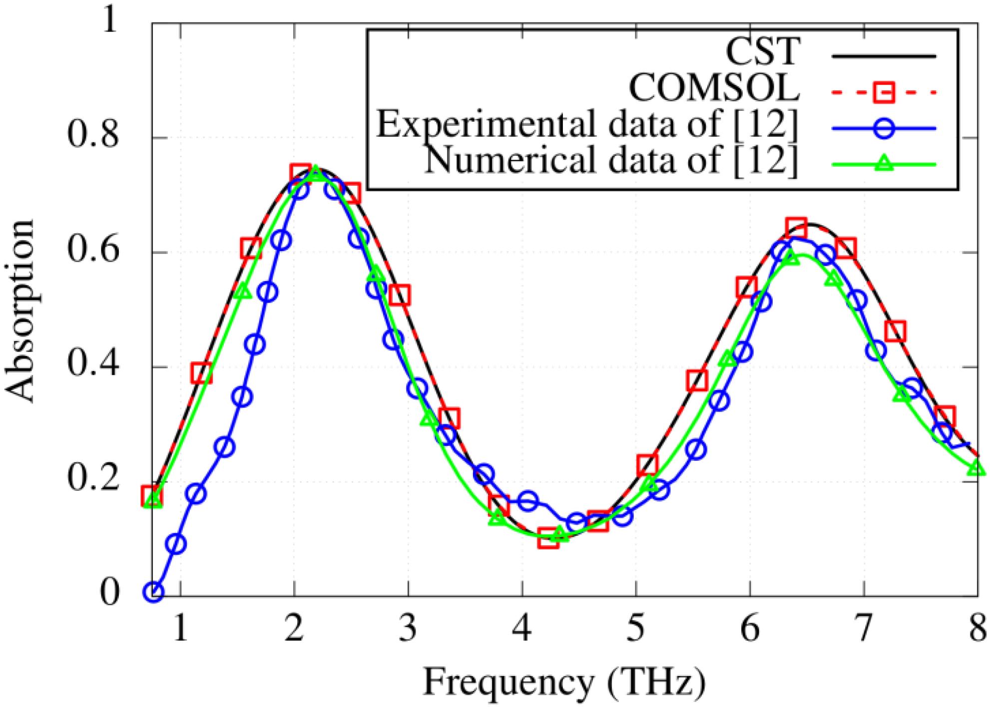
In 2019, Tasolamprou et al. conducted experiments in [1212 [12] A. C. Tasolamprou, A. D. Koulouklidis, C. Daskalaki, C. P. Mavidis, G. Kenanakis, G. Deligeorgis, Z. Viskadourakis, P. Kuzhir, S. Tzortzakis, M. Kafesaki, E. N. Economou and C. M. Soukoulis, “Experimental demonstration of ultrafast THz modulation in a graphene-based thin film absorber through negative photoinduced conductivity,” ACS photonics, vol. 6, no. 3, pp. 720-727, 2019.] regarding measurements of absorption levels of plane THz waves by a graphene sheet stacked over a lossy SU-8 substrate. Based on this set up, illustrated by Fig. 20, they produced an ultrafast optically tunable THz modulator.
Schematic diagram of the experiment conducted in [1212 [12] A. C. Tasolamprou, A. D. Koulouklidis, C. Daskalaki, C. P. Mavidis, G. Kenanakis, G. Deligeorgis, Z. Viskadourakis, P. Kuzhir, S. Tzortzakis, M. Kafesaki, E. N. Economou and C. M. Soukoulis, “Experimental demonstration of ultrafast THz modulation in a graphene-based thin film absorber through negative photoinduced conductivity,” ACS photonics, vol. 6, no. 3, pp. 720-727, 2019.] for measuring graphene absorption of THz incident wave.
In this appendix, we have numerically reproduced the setup of Fig. 20 using the commercial simulators CST and COMSOL and the absorption levels of incident THz waves have been calculated. As in [1212 [12] A. C. Tasolamprou, A. D. Koulouklidis, C. Daskalaki, C. P. Mavidis, G. Kenanakis, G. Deligeorgis, Z. Viskadourakis, P. Kuzhir, S. Tzortzakis, M. Kafesaki, E. N. Economou and C. M. Soukoulis, “Experimental demonstration of ultrafast THz modulation in a graphene-based thin film absorber through negative photoinduced conductivity,” ACS photonics, vol. 6, no. 3, pp. 720-727, 2019.], the graphene sheet was subjected to the chemical potential μc = 0.25 eV. The chemical vapor deposition (CVD-grown) technique was employed, producing transport relaxation time τ = 25 fs for the graphene sheet [1212 [12] A. C. Tasolamprou, A. D. Koulouklidis, C. Daskalaki, C. P. Mavidis, G. Kenanakis, G. Deligeorgis, Z. Viskadourakis, P. Kuzhir, S. Tzortzakis, M. Kafesaki, E. N. Economou and C. M. Soukoulis, “Experimental demonstration of ultrafast THz modulation in a graphene-based thin film absorber through negative photoinduced conductivity,” ACS photonics, vol. 6, no. 3, pp. 720-727, 2019.]. Also, due to the used fabrication technique, the real part of the graphene conductivity is 70% greater than that predicted by the theory for a perfect sheet, given by (1)–(4) [1212 [12] A. C. Tasolamprou, A. D. Koulouklidis, C. Daskalaki, C. P. Mavidis, G. Kenanakis, G. Deligeorgis, Z. Viskadourakis, P. Kuzhir, S. Tzortzakis, M. Kafesaki, E. N. Economou and C. M. Soukoulis, “Experimental demonstration of ultrafast THz modulation in a graphene-based thin film absorber through negative photoinduced conductivity,” ACS photonics, vol. 6, no. 3, pp. 720-727, 2019.]. The SU-8 substrate is 19 μm in thickness and its relative complex permittivity is εr = 3.9 + j0.089. The imaginary part of εr was calibrated in this paper for properly modeling the losses of the substrate, as long as it is not provided by the reference paper. Finally, beneath the substrate, a perfect electrical conductor (PEC) slab acts as a ground plane for the structure.
In CST and COMSOL, the structure is excited by a TM mode (p-polarization) plane wave, of which angle of incidence is θi = 45° (Fig. 20), such as indicated in [1212 [12] A. C. Tasolamprou, A. D. Koulouklidis, C. Daskalaki, C. P. Mavidis, G. Kenanakis, G. Deligeorgis, Z. Viskadourakis, P. Kuzhir, S. Tzortzakis, M. Kafesaki, E. N. Economou and C. M. Soukoulis, “Experimental demonstration of ultrafast THz modulation in a graphene-based thin film absorber through negative photoinduced conductivity,” ACS photonics, vol. 6, no. 3, pp. 720-727, 2019.]. The plane wave is generated by using a Floquet port. Furthermore, periodic Floquet conditions are applied at the side ends of the domain for yielding required periodicity.
Fig. 21 shows the results of experimental measurements and numerical calculations of [1212 [12] A. C. Tasolamprou, A. D. Koulouklidis, C. Daskalaki, C. P. Mavidis, G. Kenanakis, G. Deligeorgis, Z. Viskadourakis, P. Kuzhir, S. Tzortzakis, M. Kafesaki, E. N. Economou and C. M. Soukoulis, “Experimental demonstration of ultrafast THz modulation in a graphene-based thin film absorber through negative photoinduced conductivity,” ACS photonics, vol. 6, no. 3, pp. 720-727, 2019.] and of numerical calculations of the absorption spectra obtained in this paper using COMSOL and CST. Good agreement is observed among the experimental curve and our numerical results, especially at the resonance frequencies (2.17 THz and 6.38 THz). Our numerical data is also well-matched with the calculations of [1212 [12] A. C. Tasolamprou, A. D. Koulouklidis, C. Daskalaki, C. P. Mavidis, G. Kenanakis, G. Deligeorgis, Z. Viskadourakis, P. Kuzhir, S. Tzortzakis, M. Kafesaki, E. N. Economou and C. M. Soukoulis, “Experimental demonstration of ultrafast THz modulation in a graphene-based thin film absorber through negative photoinduced conductivity,” ACS photonics, vol. 6, no. 3, pp. 720-727, 2019.]. Indirectly, our FDTD method is validated once more, as it agrees very well with COMSOL and CST results. Nevertheless, in face of the experiments conducted in [1212 [12] A. C. Tasolamprou, A. D. Koulouklidis, C. Daskalaki, C. P. Mavidis, G. Kenanakis, G. Deligeorgis, Z. Viskadourakis, P. Kuzhir, S. Tzortzakis, M. Kafesaki, E. N. Economou and C. M. Soukoulis, “Experimental demonstration of ultrafast THz modulation in a graphene-based thin film absorber through negative photoinduced conductivity,” ACS photonics, vol. 6, no. 3, pp. 720-727, 2019.] and of the validated design of the proposed smart FSS, we also may say that it is perfectly feasible to manufacture the FSS device proposed in this paper.
Comparison among absorption spectra obtained experimentally and numerically in [1212 [12] A. C. Tasolamprou, A. D. Koulouklidis, C. Daskalaki, C. P. Mavidis, G. Kenanakis, G. Deligeorgis, Z. Viskadourakis, P. Kuzhir, S. Tzortzakis, M. Kafesaki, E. N. Economou and C. M. Soukoulis, “Experimental demonstration of ultrafast THz modulation in a graphene-based thin film absorber through negative photoinduced conductivity,” ACS photonics, vol. 6, no. 3, pp. 720-727, 2019.] and the spectra calculated in this work using CST and COMSOL.
REFERENCES
-
1[1] M. Bashiri, C. Ghobadi, J. Nourinia, and M. Majidzadeh, “WiMAX, WLAN, and X-Band Filtering Mechanism: Simple-Structured Triple-Band Frequency Selective Surface,” IEEE Antennas and Wireless Propagation Letters, vol. 16, pp. 3245-3248, Nov. 2017.
-
2[2] E. S. Torabi, A. Fallahi, and A. Yahaghi, “Evolutionary Optimization of Graphene-Metal Metasurfaces for Tunable Broadband Terahertz Absorption,” IEEE Transactions on Antennas and Propagation, vol. 65, no. 3, pp. 1464-1467, Mar. 2017.
-
3[3] M. Qu et al., “Design of a Graphene-Based Tunable Frequency Selective Surface and Its Application for Variable Radiation Pattern of a Dipole at Terahertz,” Radio Science, vol. 53, no. 2, pp. 183-189, Jan. 2018.
-
4[4] K. S. Novoselov and A. K. Geim, “The Rise of Graphene,” Nat. Mater., vol. 6, no. 3, pp. 183-191, Mar. 2007.
-
5[5] G. W. Hanson, “Dyadic Green's functions and guided surface waves for a surface conductivity model of graphene,” J. Appl. Phys., vol.103, no. 6, p. 064302, Mar. 2008.
-
6[6] J. S. Gómez-Díaz and J. Perruisseau-Carrier, “Graphene-based plasmonic switches at near infrared frequencies,” Optics Express, vol. 21, no. 13, pp. 15490-15504, 2013.
-
7[7] M. Qu, M. Rao, S. Li, and L. Deng, “Tunable antenna radome based on graphene frequency selective surface,” AIP Advances, vol. 7, no. 9, p. 095307, 2017.
-
8[8] J. Chen, G. Hao, and Q. H. Liu, “Using the ADI-FDTD Method to Simulate Graphene-Based FSS at Terahertz Frequency,” IEEE Transactions on Electromagnetic Compatibility, vol. 59, no. 4, pp. 1218-1223, Aug. 2017.
-
9[9] D. W. Wang et al., “Tunable THz Multiband Frequency-Selective Surface Based on Hybrid Metal-Graphene Structures,” IEEE Transactions on Nanotechnology, vol. 16, no. 6, pp. 1132-1137, Nov. 2017.
-
10[10] L. Lin, L. S. Wu, W. Y. Yin, and J. F. Mao, “Modeling of magnetically biased graphene patch frequency selective surface (FSS),” in 2015 IEEE MTT-S International Microwave Workshop Series on Advanced Materials and Processes for RF and THz Applications (IMWS-AMP), Jul. 2015, pp. 1-3.
-
11[11] P. K. Khoozani, M. Maddahali, M. Shahabadi, and A. Bakhtafrouz, “Analysis of magnetically biased graphene-based periodic structures using a transmission-line formulation,” J. Opt. Soc. Am. B, vol. 33, no. 12, pp. 2566-2576, Dec. 2016.
-
12[12] A. C. Tasolamprou, A. D. Koulouklidis, C. Daskalaki, C. P. Mavidis, G. Kenanakis, G. Deligeorgis, Z. Viskadourakis, P. Kuzhir, S. Tzortzakis, M. Kafesaki, E. N. Economou and C. M. Soukoulis, “Experimental demonstration of ultrafast THz modulation in a graphene-based thin film absorber through negative photoinduced conductivity,” ACS photonics, vol. 6, no. 3, pp. 720-727, 2019.
-
13[13] X. H. Wang, W. Y. Yin, and Z. Chen, “Matrix Exponential FDTD Modeling of Magnetized Graphene Sheet,” IEEE Antennas and Wireless Propagation Letters, vol. 12, pp. 1129-1132, 2013.
-
14[14] ANSYS. HFSS. [Online]. Available: ansys.com/products/electronics.
» ansys.com/products/electronics -
15[15] R. M. S. de Oliveira, N. R. N. M. Rodrigues and V. Dmitriev, “FDTD Formulation for Graphene Modeling Based on Piecewise Linear Recursive Convolution and Thin Material Sheets Techniques,” IEEE Antennas and Wireless Propagation Letters, vol. 14, pp. 767-770, 2015.
-
16[16] D. L. Sounas and C. Caloz, “Gyrotropy and Nonreciprocity of Graphene for Microwave Applications,” IEEE Transactions on Microwave Theory and Techniques, vol. 60, no. 4, Apr. 2012.
-
17[17] P. Gonçalves and N. Peres, An Introduction to Graphene Plasmonic. World Scientific, 2016, ch. 3, pp 47-66.
-
18[18] Ž. i. Kancleris, G. Slekas, and A. Matulis, “Modeling of Two-Dimensional Electron Gas Sheet in FDTD Method,” IEEE Transactions on Antennas and Propagation, vol. 61, no. 2, pp. 994–996, Feb. 2013.
-
19[19] D. Y. Heh and E. L. Tan, “FDTD Modeling for Dispersive Media Using Matrix Exponential Method,” IEEE Microwave and Wireless Components Letters, vol. 19, no. 2, pp. 53–55, Feb. 2009.
-
20[20] A. Taflove and S. C. Hagness, “Introduction to Maxwell’s Equations and the Yee algorithm, Incident Wave Source Conditions,” in Computational Electrodynamics: The Finite-Difference Time-Domain Method. Norwood, MA, USA: Artech House, 2005, ch. 3,5, pp. 58–79,186–201.
-
21[21] J. Maloney and G. Smith, “The efficient modeling of thin material sheets in the finite-difference time-domain (FDTD) method,” IEEE Transactions on Antennas and Propagation, vol. 40, no. 3, pp. 323–330, Mar 1992.
-
22[22] J. A. Roden and S. D. Gedney, “Convolution PML (CPML): An efficient FDTD implementation of the CFS-PML for arbitrary media,” Microwave and Optical Tech. Letters, vol. 27, no. 5, pp. 334–339, 2000.
-
23[23] F. Yang, J. Chen, R. Qiang, and A. Elsherbeni, “A simple and efficient FDTD/PBC algorithm for scattering analysis of periodic structures,” Radio Science, vol. 42, no. 4, pp. 1–9, Aug. 2007.
Publication Dates
-
Publication in this collection
11 Nov 2019 -
Date of issue
Oct-Dec 2019
History
-
Received
27 Mar 2019 -
Reviewed
28 Mar 2019 -
Accepted
04 July 2019