
Abstract
In this paper, a novel method is proposed to increase the gain and radiation efficiency of a compact patch antenna. By employing a combination of three efficient techniques, we have developed a multi-resonance L-DGS antenna with a high gain of 5 dB and an efficiency of 99.6%. Furthermore, a novel compact Double Negative metamaterial unit cell and its equivalent circuit are investigated, to achieve high miniaturization of 30×30 mm2 and multi-band wireless applications (2.8 GHz, 4.1-4.45 GHz, 5.6 GHz). Koch snowflake fractal is introduced along radiation patch edges to improve the antenna matching. The antenna is designed using commercially available package CST software, printed on Rogers RT5880, and the probe feed mechanism is adopted for the antenna excitation. Then, to prove the validation of the antenna design, the equivalent circuit is presented and simulated using ADS of Agilent software. The compared simulation results given by CST, HFSS and ADS software have confirmed the antenna use for WIMAX, C-band and WLAN applications.
Index Terms
Compact antenna; Miniaturisation; Metamaterials; Fractal technique; DGS technique
I. INTRODUCTION
Man’s modern life is characterized by the wide use of electronic mobile devices. For their efficient and optimal use, they must be compact and able of multifunction and multi-frequency band operation that corresponds to the standards such as IEEE 806.16, IEEE 806.11, GSM, CDMA, etc. Communication standards, e.g., Bluetooth, WIFI, ZigBee, WiMAX, mobile networks have been developing too fast, which require the integration of one or more antennas in one unit. To satisfy this requirement, the antenna, in particular, must be conformal to the device body, compact in size, and able to operate at multiple frequencies of mobile communication systems. As an example of such use, modern electrocardiography (ECG) monitors, blood pressure monitors, and biosensors in the medical field, which are going through the telecommunications field and making use of GPS devices, cell phones, and smart wearable, etc. Facing this technological challenge, research works on small antenna construction have naturally been developed. Several techniques have already been proposed during past decades. Even so, these techniques have the inconvenient to decrease the antenna performance’s in most cases. So, at present, designing a compact antenna with good performances and ability of integration into small volumes presents a real challenge.
Broadly speaking, there are two different categories of miniaturization methods, each of which contains several techniques. The first category is based on the extension of the electrical current path by the modification of the geometry. One of the widely used techniques that reduce the antenna space is meander line [1[1] J. L. Volakis, C.-C. Chen, and K. (Kyõhei) Fujimoto, Small antennas: miniaturization techniques & applications. McGraw-Hill, 2010.]. However, although it allows size compactness, this technique most often results in antennas with narrower bandwidth [2[2] N. Michishita, Y. Yamada, and N. Nakakura, “Miniaturization of a small meander line antenna by loading a high εr material,” in 2004 Joint Conference of the 10th Asia-Pacific Conference on Communications and the 5th International Symposium on Multi-Dimensional Mobile Communications Proceedings, APCC/MDMC’04, 2004, vol. 2, pp. 651–654, doi: 10.1109/apcc.2004.1391796.
https://doi.org/10.1109/apcc.2004.139179...
]. Another proposed technique is fractal geometries [3[3] S. R. Best and J. D. Morrow, “The effectiveness of space-filling fractal geometry in lowering resonant frequency,” IEEE Antennas Wirel. Propag. Lett., vol. 1, no. 1, pp. 112–115, 2002, doi: 10.1109/LAWP.2002.806050.
https://doi.org/10.1109/LAWP.2002.806050...
]–[5[5] R. Azaro, G. Boato, M. Donelli, G. Franceschini, A. Martini, and A. Massa, “Design of miniaturised ISM-band fractal antenna,” Electron. Lett., vol. 41, no. 14, pp. 785–786, Jul. 2005, doi: 10.1049/el:20050774.
https://doi.org/10.1049/el:20050774...
], which increases the current path. Consequently, a reduction of the physical dimension is achieved. Besides, this technique has proven its efficacy in designing multiband structures with more economical low profile [6[6] W. L. Chen and G. M. Wang, “Small size edge-fed Sierpinski carpet microstrip patch antennas,” Prog. Electromagn. Res. C, vol. 3, pp. 195–202, 2008, doi: 10.2528/PIERC08050302.
https://doi.org/10.2528/PIERC08050302...
]. The self-similarity of the fractal geometries provides impedance matching at multiple operating bands. Therefore, impedance matching is achieved by two types of methods, structural modification and lumped elements insertion [7[7] T. C. Edwards and M. B. Steer, Foundations of Interconnect and Microstrip Design. West Sussex, England: John Wiley & Sons, Ltd, 2000.]–[9[9] W.-K. Chen, “Theory and Design of Broadband Matching Networks – 1st Edition,” 1976. https://www.elsevier.com/books/theory-and-design-of-broadband-matching-networks/chen/978-0-08-019702-9 (accessed Aug. 30, 2020).
https://www.elsevier.com/books/theory-an...
]. Many papers have used the fractal technique to enhance the impedance matching of the antenna [10[10] R. Kumar and P. N. Chaubey, “On the design of tree-type ultra wideband fractal antenna for DS-CDMA system,” J. Microwaves, Optoelectron. Electromagn. Appl., vol. 11, no. 1, pp. 107–121, Jun. 2012, doi: 10.1590/S2179-10742012000100009.
https://doi.org/10.1590/S2179-1074201200...
]–[12[12] H. Rmili, J. M. Floch, and H. Zangar, “Experimental study of a 2-D irregular fractal-jet printed antenna,” IEEE Antennas Wirel. Propag. Lett., vol. 8, pp. 328–331, 2009, doi: 10.1109/LAWP.2009.2015223.
https://doi.org/10.1109/LAWP.2009.201522...
]. However, the bandwidth as well as the efficiency of the Koch fractal monopole antenna has exceedingly degraded compared to the monopole antenna [13[13] C. P. Baliarda, C. B. Borau, M. N. Rodero, and J. R. Robert, “An iterative model for fractal antennas: Application to the Sierpinski gasket antenna,” IEEE Trans. Antennas Propag., vol. 48, no. 5, pp. 713–719, 2000, doi: 10.1109/8.855489.
https://doi.org/10.1109/8.855489...
]. Another commonly used technique for printed antennas is the introduction of shortening pin for the purposes of miniaturization. This technique can provide a compact size to a maximum of wavelength quarter, though; the slots can distort the radiation patterns [14[14] G. Zhou, “Shorting-pin loaded annular ring microstrip antenna,” in IEEE Antennas and Propagation Society International Symposium, 1998 Digest - Antennas: Gateways to the Global Network - Held in conjunction with: USNC/URSI National Radio Science Meeting, 1998, vol. 2, pp. 900–903, doi: 10.1109/APS.1998.702094.
https://doi.org/10.1109/APS.1998.702094...
]. Besides compactness, this technique is practical to any antenna form. Slot-loading technique is one of the promising techniques, which is also reported in the literature. Interesting slots to the radiating metallic results have been obtained in reducing the size of a patch antenna and producing multiband operation within a specified frequency range [15[15] R. H. Chen and Y. C. Lin, “Miniaturized design of microstrip-fed slot antennas loaded with C-shaped rings,” IEEE Antennas Wirel. Propag. Lett., vol. 10, pp. 203–206, 2011, doi: 10.1109/LAWP.2011.2123075.
https://doi.org/10.1109/LAWP.2011.212307...
]. Ground plan modification or so-called Defected Ground Technique (DGS) is another method for planar antennas miniaturisation [16[16] X. Cheng, D. E. Senior, C. Kim, and Y. K. Yoon, “A compact omnidirectional self-packaged patch antenna with complementary split-ring resonator loading for wireless endoscope applications,” IEEE Antennas Wirel. Propag. Lett., vol. 10, pp. 1532–1535, 2011, doi: 10.1109/LAWP.2011.2181315.
https://doi.org/10.1109/LAWP.2011.218131...
], the reduction of ground plan size or inserting slots in the ground plan helps in lowering the operating frequency, which leads to size reduction, except, this technique has drawbacks of increasing the back-lob level. The addition of reactive components to slot antennas is considered as a method of miniaturization [17[17] A. Alù, F. Bilotti, N. Engheta, and L. Vegni, “Subwavelength, compact, resonant patch antennas loaded with metamaterials,” IEEE Trans. Antennas Propag., vol. 55, no. 1, pp. 13–25, Jan. 2007, doi: 10.1109/TAP.2006.888401.
https://doi.org/10.1109/TAP.2006.888401...
]. In [18[18] C. S. Hong, “Small annular slot antenna with capacitor loading,” Electron. Lett., vol. 36, no. 2, pp. 110–111, Jan. 2000, doi: 10.1049/el:20000147.
https://doi.org/10.1049/el:20000147...
], with the use of chip capacitor loading, Cheng-Shong Hong has achieved a 23.4 % slot antenna area size reduction. Unfortunately, the common disadvantage of such antennas is the high-quality factor, which occurs from the capacitor loading. The second category of miniaturization is based on manipulating the dielectric and magnetic properties of the antenna material. Generally speaking, this method includes three different techniques. The first one consists of using substrates with high permittivity, typically of 10 to 20 order. Thus, this class substrate allows reducing the antenna size with no geometry changing [19[19] Y. Hwang, Y. P. Zhang, G. X. Zheng, and T. K. C. Lo, “Planar inverted F antenna loaded with high permittivity material,” Electron. Lett., vol. 31, no. 20, pp. 1710–1712, Sep. 1995, doi: 10.1049/el:19951184.
https://doi.org/10.1049/el:19951184...
]. The main drawback of this technique remains in the high cost of the substrates during the manufacturing process. The second solution that was increasingly attracting research attention over the last few years is employing the magnetoelectric (ME) materials. The ME coupling effect brings novel functionalities to develop many new types of electronics such as high-speed memory, radio frequency resonator, compact ME antenna, and weak magnetic field sensors [20[20] Y. Cheng, B. Peng, Z. Hu, Z. Zhou, and M. Liu, “Recent development and status of magnetoelectric materials and devices,” Phys. Lett. Sect. A Gen. At. Solid State Phys., vol. 382, no. 41, pp. 3018–3025, Oct. 2018, doi: 10.1016/j.physleta.2018.07.014.
https://doi.org/10.1016/j.physleta.2018....
]. On the practical side, most existing ME materials have both high permittivity and permeability with many losses. Also, the limited commercial EM materials are only usable for frequencies up to 1 GHz and are of a high cost [21[21] C. Niamien, S. Collardey, A. Sharaiha, and K. Mahdjoubi, “Surface wave loss and material loss in printed antennas over magneto-dielectric materials,” in 2010 14th International Symposium on Antenna Technology and Applied Electromagnetics and the American Electromagnetics Conference, ANTEM/AMEREM 2010, 2010, doi: 10.1109/ANTEM.2010.5552498.
https://doi.org/10.1109/ANTEM.2010.55524...
-22[22] F. Canneva et al., “Miniature reconfigurable antenna with magneto dielectric substrate for DVB-H band,” Microw. Opt. Technol. Lett., vol. 55, no. 9, pp. 2007–2011, Sep. 2013, doi: 10.1002/mop.27793.
https://doi.org/10.1002/mop.27793...
]. The alternative solution to design electrical circuits, compact antennas in particular with novel properties like small profile, low losses, is the use of artificial electromagnetic materials, also known as metamaterials. This specific class of materials has proven to be a universal and very powerful technique of miniaturization [23[23] K. Li, C. Zhu, L. Li, Y. M. Cai, and C. H. Liang, “Design of electrically small metamaterial antenna with ELC and EBG loading,” IEEE Antennas Wirel. Propag. Lett., vol. 12, pp. 678–681, 2013, doi: 10.1109/LAWP.2013.2264099.
https://doi.org/10.1109/LAWP.2013.226409...
]. Unlike many other techniques, Metamaterials do not lower the bandwidth of the antenna.
Despite the miniaturisation possibilities granted by the mentioned techniques, they usually come to a compromise of size, bandwidth, and radiation efficiency. To overcome this issue, a combination of multiple miniaturisation techniques can reduce these drawbacks. Varamini et al. have designed a compact microstrip antenna with dual-band characteristics by blending of the metamaterial and fractal techniques, where a slot antenna is developed with Sierpinski carpet and Minkowski fractals, and then a metamaterial unit cell is loaded on the slot area of the antenna. The proposed antenna showed two resonances frequencies at 3.2 and 4.5 GHz [24[24] G. Varamini, A. Keshtkar, N. Daryasafar, and M. Naser-Moghadasi, “Microstrip Sierpinski fractal carpet for slot antenna with metamaterial loads for dual-band wireless application,” AEU - Int. J. Electron. Commun., vol. 84, pp. 93–99, Feb. 2018, doi: 10.1016/j.aeue.2017.11.028.
https://doi.org/10.1016/j.aeue.2017.11.0...
]. Furthermore, the authors have proposed slight modification to the metamaterial layer and introduced reconfigurable qualification, where both resonances are shifted to 3.5 and 5.8 GHz. Against the background of miniaturisation techniques combining, by adopting defected ground structure (DGS), metamaterial cell and interdigital capacitor (IDC) shaped slots, Singh, Amit Kumar, et al. have designed a miniaturized significant gain triple-band patch antenna [25[25] A. K. Singh, M. P. Abegaonkar, and S. K. Koul, “Miniaturized multiband microstrip patch antenna using metamaterial loading for wireless application,” Prog. Electromagn. Res. C, vol. 83, pp. 71–82, 2018, doi: 10.2528/pierc18012905.
https://doi.org/10.2528/pierc18012905...
]. Initially, a patch antenna resonates at 10.15 GHz is designed, and then the radiating patch is loaded with IDC to add a series capacitance, which decreased the resonance frequency to 7.57 GHz. Further, a modified double circular slot ring resonator (MDCSRR) is inserted as a DGS; this caused a significant shift in resonant frequency to 3.20 GHz, resulting in miniaturization of 68.83%. Besides a triple band of operation with a gain of 3.28 dBi at 3.2 GHz, 2.76 dBi at 5.4 GHz and 3.1 dBi at 5.8 GHz. The shorting vias and slots were combined by Boukarkar, X. Lin et al. in [26[26] A. Boukarkar, X. Q. Lin, Y. Jiang, and Y. Q. Yu, “Miniaturized Single-Feed Multiband Patch Antennas,” IEEE Trans. Antennas Propag., vol. 65, no. 2, pp. 850–854, Feb. 2017, doi: 10.1109/TAP.2016.2632620.
https://doi.org/10.1109/TAP.2016.2632620...
], to design a miniaturized multi-band patch antenna. A size reduction of 60% is achieved by loading metallic shorting vias on the edge of the radiating patch, while the multi resonance is obtained by etching multiple inverted U-shapes slots. Peak gains and efficiencies vary from 1.43–3.06 dBi and 42–74%, respectively are measured.
This paper presents an efficient method for miniaturisation techniques combination to obtain a multi-resonance antenna with a very compact size and high gain and efficiency. In addition to that, a new approach for designing multi resonant metamaterial unit cell is developed and presented. Two newly modified-CSRRs are integrated into a single layer, to achieve a unit cell design with the desired characteristics. Moreover, the designed unit cell is engraved on the radiating patch of a microstrip antenna to achieve high miniaturisation and triple frequency band of operation. For further improvement in impedance matching, the third iteration of Koch-snowflake fractal is introduced along the four edges of the radiating patch, and the ground plan is defected with an L-shaped slot to increase the gain and efficiency of the antenna.
This study is achieved in four stages. In the first stage, we present the design methodology and simulation results of the new modified CSRR unit cell. In the second stage, the new designed MTM unit cell is engraved in the resonating patch of a conventional coaxial feed printed antenna, to attain the multi resonance and reduce size. Then, the Koch snowflake fractal is introduced along the edges of the square patch to improve impedance matching, named stage three. Finally, L-shaped slot is etched from the ground plan centre, to enhance the radiation properties, besides the return loss.
II. GEOMETRY AND PERFORMANCE OF METAMATERIAL UNIT CELL
The proposed metamaterial unit cell developing method proposed in this paper starts with designing a conventional complementary split ring resonator as a reference. The analysis of the reference unit cell geometries and results lead to understanding the effect of every parameter. From this background, the Single Diagonal CSRR (SDCSRR) unit cell in Fig. 1(a) is designed by introducing an additional split and a diagonal to the original CSRR to introduce a dual resonance at a lower frequency. Further, the SDCSRR size is reduced, then, a cross-diagonal and a split are inserted as in Fig.1 (b), to swipe up the resonance frequency to the upper WLAN 5 GHz range. In a final step, the SDCSRR and CDCSRR metamaterials cells are combined into a single SCDCSRR cell layer (Fig. 1(c)) that gathers the characteristics of both unit cells. Fig. 1(f) describes in details the design methodology of the proposed unit cell SCDCSRR. The unit cells dimensions are given in Table I. The Rogers 5880RT substrate of a dielectric constant of 2.2, a loss tangent of 0.0009, and a thickness of 3.175 is considered for this study. The unit cells are enclosed in an air-filled waveguide, excited by two waveguide ports perpendicular to the Y-axis, while the Perfect Electric Conductor PEC and Perfect Magnetic Conductor PMC are assigned to the X and Z axis, respectively, as depicted in figure 1 (d). The CST Microwave Studio software is used to design the metamaterial unit cells and retrieve the scattering parameters. The metamaterial structures could be measured by connecting the unit cells into an AgilentTM PNA-L Series Network Analyzer using SMA ports and co-axial cables to find the S-parameters, as in Fig. 1(e).

Geometry of (a) Single Diagonal CSRR, (b) Cross Diagonal CSRR, (c) Integrated SCDCSRR cell, (d) Boundaries conditions, (e) measurement method, and (f) Design methodology of the proposed SCDCSRR cell.
The Single Diagonal Complementary Split Ring Resonator SDCSRR is designed by introducing an additional split and a diagonal to the conventional CSRR. The split gap has a capacitance effect, as expressed in equation (1) [27[27] R. Selvaraju, M. H. Jamaluddin, M. R. Kamarudin, J. Nasir, and M. H. Dahri, “Complementary split ring resonator for isolation enhancement in 5G communication antenna array,” Prog. Electromagn. Res. C, vol. 83, pp. 217–228, Jan. 2018, doi: 10.2528/pierc18011019.
https://doi.org/10.2528/pierc18011019...
].
Where ε0 is the permittivity of free space, T1 and t present the width and thickness of the rings, respectively. The total capacitance is the mean of the series capacitance CS and the gap capacitance Cg.
The diagonal increases the wire length, so it has an inductance effect which is calculated by equation (2) as follows [28[28] I. Bahl and P. Bhartia, Microwave solid state circuit design, vol. 26, no. 02. 2003.]–[30[30] C. R. Paul, Inductance: Loop and Partial. 2009.]:
The parameter l presents the length of the microstrip line and it is calculated by l = 2(4 W1 + √2 W1) – 2G1, where w and t are the thickness and the width of the microstrip line, respectively. Kg is the correction factor and it is calculated by the equation , here ‘ is the width and h’ is the thickness of the substrate.
The resonance frequency can be calculated by:
The equivalent circuit is a qualitative response from the structure, used to understand or predict the resonance mechanism of an electrical circuit at respective resonant frequencies [31[31] D. H. Johnson, “Origins of the equivalent circuit concept: The voltage-source equivalent,” Proceedings of the IEEE, vol. 91, no. 4. Institute of Electrical and Electronics Engineers Inc., pp. 636–640, 2003, doi: 10.1109/JPROC.2003.811716.
https://doi.org/10.1109/JPROC.2003.81171...
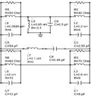
]. The equivalent circuit of the unit cell presented in Fig. 2 is constructed with the help of a shunt connected resonators comprised of capacitors and inductors, both arranged in series and/or in parallel. The given lumped elements values are calculated using the Advanced Design System (ADS) software.

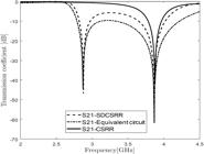
As shown in Fig. 3, the SDCSRR transmission coefficient over the frequency band from 2 to 4.5 GHz, presents a low resonance frequency at 2.8 GHz, in addition to the resonance frequency of the conventional CSRR at 3.7 GHz. According to the obtained results, the performance of the SDCSRR design method is validated. The S21 equivalent circuit curve agrees well with the CST result.
To generate a frequency of operation at the upper WLAN band (5 GHz), firstly, SDCSRR size is reduced, then, a second diagonal is introduced to design the Cross Diagonal CSRR (CDCSRR). The parametric study of the CDCSRR unit cell dimensions effects on the resonance frequency is investigated and presented in table II. The equivalent circuit and lumped elements values are presented in Fig. 4.

From Fig. 5, CDCSRR transmission coefficient presents a resonance frequency at 5 GHz with impedance matching of -68 dB. Also, an excellent matching with S21 of the equivalent circuit is observed.


The SDCSRR and CDCSRR unit cells are combined into a single layer metamaterial unit cell (SCDCSRR), to gather the properties of both previous unit cells. Fig. 7 shows a comparison between the transmission coefficients of the final unit cell structure with two CDCSRRs in the centre and the upper right corner of the SDCSRR, the SDCSRR cell with a single CDCSRRSS in the centre, and the equivalent circuit of the final unit cell.
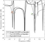
The S21 comparison presents three resonance frequencies 2.8 GHz, 4 GHz and 5GHs, respectively. The additional CDCSRR at the upper right corner has improved the impedance matching at 5GHz and reducing the unwanted harmonics at 5.8 GHz without need of an additional filter component.
A Matlab code based on the equations (5–8) is used to retrieve the electromagnetic properties of the unit cells [32[32] Z. Szabó, G. H. Park, R. Hedge, and E. P. Li, “A unique extraction of metamaterial parameters based on Kramers-Kronig relationship,” IEEE Trans. Microw. Theory Tech., vol. 58, no. 10, pp. 2646–2653, Oct. 2010, doi: 10.1109/TMTT.2010.2065310.
https://doi.org/10.1109/TMTT.2010.206531...
], [33[33] X. Chen, T. M. Grzegorczyk, B.-I. Wu, J. Pacheco, and J. A. Kong, “Robust method to retrieve the constitutive effective parameters of metamaterials,” doi: 10.1103/PhysRevE.70.016608.
https://doi.org/10.1103/PhysRevE.70.0166...
]. The impedance z is calculated using the scattering parameters S11 and S21 extracted from CST microwave studio.
The refractive index n is dependent on the scattering parameters, the dielectric slab thickness d, and the wave victor in free space k.
Then the permittivity and permeability can be calculated as follows:
And
The transmission coefficient phase of the SDCSRR in Fig. 8 shows a phase variation of 180° at 2.8 GHz, which explain the appearance of the negative epsilon region at this frequency. The permittivity of the CDCSRR unit cell in Fig. 9 shows a negative region at 5GHz; thus, the ENG characteristic is confirmed. Fig. 10 presents the permittivity of the SCDCSRR unit cell, the SCDCSRR configuration with two CDCSRR unit cells has two epsilon negative regions around 2.8 GHz and 5 GHz; thus, it carries the metamaterial properties of both the SDCSRR and CDCSRR unit cells.


Table III resumes the characteristics of the three simulated unit cells.
III. ANTENNA DESIGN AND METAMATERIAL LOADING
The proposed antenna design is based on the conventional rectangular patch antenna [34[34] W. F. Richards, “Microstrip Antennas,” in Antenna Handbook, Springer US, 1988, pp. 639–712.]. the dimensions of the reference antenna are calculated using the following equations (9–11) [35[35] C. A. Balanis, Antenna theory: analysis and design. wiley, 2015.].
Where
The Rogers RT5880 substrate with a relative permittivity εeff of 2.2 and a thickness h of 3.175 mm is considered for the study. The calculated dimensions of the radiating patch for 2.5 GHz operating frequency, are 38.62 mm× 47.43 mm×3.175 mm. The coaxial feeding technique is used to feed the proposed antenna with 50-ohm impedance.
To reduce the antenna size and introduce the multi resonance, the radiation patch of the reference antenna radiation patch is miniaturized to 28 mm ×28 mm, then the proposed SCDCSRR unit cell is engraved on its centre as shown in Fig. 11.
The return loss in Fig. 12 shows that the reference antenna with 28 mm ×28 mm patch has a single resonance frequency at 3.4 GHz. By loading the SCDCSRR to the radiating patch, the unit cell has induced two resonances at 2.65 GHz and 5.2 GHz, besides improving the impedance matching at 3.4 GHz.

Return loss of conventional miniaturized antenna and that of miniaturised antenna with SCDCSRR unit cell.
Noting that the resonance frequencies locations of the antenna with metamaterial can be predicted since they match those of the SCDCSRR cell in fig.7.
The antenna size can be miniaturised whether by reducing the size and maintain the same resonance frequency or by shifting the resonance to a lower frequency and maintain the same size of the antenna [1[1] J. L. Volakis, C.-C. Chen, and K. (Kyõhei) Fujimoto, Small antennas: miniaturization techniques & applications. McGraw-Hill, 2010.]. In this paper, the proposed antenna size is miniaturized by 63.11% in two steps. First, the size of the radiating patch of the reference antenna is reduced from 38.62 mm ×47.43 mm to 28 mm ×28 mm, which resulted in a resonance frequency shift from 2.5 to 3.4 GHz. Then to attain a resonance at a lower frequency, the SCDCSRR unit cell is loaded to the radiation patch, and a resonance frequency is created at 2.65 GHz. The table IV depicts the miniaturisation process followed in this paper.
IV. FRACTAL TECHNIQUE EMPLOYING
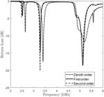
Koch snowflake fractal is etched from the four edges of the resonating patch to improve return loss at the resonance frequencies, as depicted in Fig. 13. The first order is formed of four sections, each section is one third the length of the rectangular patch (28 mm/3). In the second order, each of the four sections is replaced with the same shape which makes them sixteen segments, each one is one-ninth the patch side length. Table V resumes the effect of Koch snowflake fractal order on the antenna return loss.

V. DGS TECHNIQUE EMPLOYING
To improve the radiation parameters as gain, radiation pattern and efficiency, the DGS technique is employed. The L shaped slot is etched from the ground plan of the proposed antenna. The slot has the dimensions of GY=20 mm, GX=17mm, gy=10mm, and gx=9mm. The final antenna is fed by the SMA connector attached, as shown in Fig. 15.

The return loss of the proposed antenna is presented in Fig. 17, the DGS technique enhanced noticeably the impedance matching of the first resonance frequency, but also has shifted upward the three resonance frequencies.

Moreover, the ANSYS HFSS software is investigated to validate the CST obtained results and then, the equivalent circuit is provided. The comparison of return loss results is shown in table VI, the three return loss results show good agreement at the whole frequency ranges.
To explain the physical mechanism of radiation at the three resonance frequencies, the current distribution besides the radiation pattern are presented in Fig. 18. The distribution of surface current at the frequency 2.8 GHz is mainly concentrated in the SDCSRR and the central CDCSRR unit cells with a maximum of 530.3 A/m, as shown in Fig. 18(a). Moreover, the antenna has a two-sided radiation pattern, the forward lob at the Z-axis is more significant with a maximum gain of 5.01 dB. In Fig. 18(b), the current at the second resonance frequency is distributed at all the surface of the radiating patch, which reduces the surface current maximum to 143.7 A/m. The radiation pattern at 4.2 GHz is bidirectional with a maximum gain of 4.21 dB at the main lob in the Z-axis. Fig. 18(c) shows that the resonance frequency at 5.6 GHz is caused by the CDCSRR at upper left corner. The maximum surface current is 1030 A/m, the radiation pattern at 5.6 GHz has a main lob with a maximum gain of 5.09 dB.
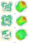
Current distribution and radiation pattern of proposed antenna at (a) 2.8 GHz, (b) 4.3 and (c) 5.6 GHz.
Fig. 19 shows that the proposed antenna provides an excellent simulated radiation efficiency with values of 96.06%, 99.3% and 95.91% at the frequencies 2.8 GHz, 4.2 GHz, and 5.6 GHz, respectively.

The methodology of input impedance measurements and pattern measurements such as gain, beamwidth, polarization, and minor lobe level of the proposed antenna are described in [36[36] L. V. Blake and M. W. Long, Antennas: Fundamentals, design, measurement, third edition. Institution of Engineering and Technology, 2009.].
In table VII, a comparative analysis is provided with respect to existing reported antennas. The comparison is made by taking into consideration the miniaturisation techniques, the overall dimension of the antennas, resonance frequency, and the gain.
VI. CONCLUSION
This paper presents a compact triple-band antenna for WIMAX and WLAN applications. The proposed antenna is designed by combining the metamaterials, fractals, and DGS. The antenna size is reduced into 63% by introducing a novel modified CSRR unit cell in the centre of a rectangular radiating patch, then, the return loss and the radiation properties are improved by employing the Koch snowflake fractal and the DGS techniques. The antenna is designed on a Rogers RT5880 substrate with an overall dimension of 30×30 mm2 and fed by a 50-ohm coaxial line. The suggested antenna is analysed using full-wave electromagnetic solvers, CST Microwave Studio (MWS), and Ansoft HFSS for validating the obtained simulated results. Moreover, the Advanced Design System (ADS) software is used to calculate the equivalent circuit of the metamaterial unit cells. The obtained results show that the proposed antenna achieves good impedance matching at the three resonating bands 2.7 GHz, 4.1-4.45 GHz, and 5.6 GHz, with a good gain of 5.01 dB, 5.21 dB and 5.09 dB, respectively, and excellent radiation efficiency of 99.6%. The comparison table proves that the proposed antenna has a smaller size, and better gain and efficiency comparing to recent multi-resonance antennas, reported in the literature.
References
-
[1]J. L. Volakis, C.-C. Chen, and K. (Kyõhei) Fujimoto, Small antennas: miniaturization techniques & applications McGraw-Hill, 2010.
-
[2]N. Michishita, Y. Yamada, and N. Nakakura, “Miniaturization of a small meander line antenna by loading a high εr material,” in 2004 Joint Conference of the 10th Asia-Pacific Conference on Communications and the 5th International Symposium on Multi-Dimensional Mobile Communications Proceedings, APCC/MDMC’04, 2004, vol. 2, pp. 651–654, doi: 10.1109/apcc.2004.1391796.
» https://doi.org/10.1109/apcc.2004.1391796 -
[3]S. R. Best and J. D. Morrow, “The effectiveness of space-filling fractal geometry in lowering resonant frequency,” IEEE Antennas Wirel. Propag. Lett., vol. 1, no. 1, pp. 112–115, 2002, doi: 10.1109/LAWP.2002.806050.
» https://doi.org/10.1109/LAWP.2002.806050 -
[4]J. P. Gianvittorio and Y. Rahmat-Samii, “Fractal antennas: A novel antenna miniaturization technique, and applications,” IEEE Antennas Propag. Mag., vol. 44, no. 1, pp. 20–36, Feb. 2002, doi: 10.1109/74.997888.
» https://doi.org/10.1109/74.997888 -
[5]R. Azaro, G. Boato, M. Donelli, G. Franceschini, A. Martini, and A. Massa, “Design of miniaturised ISM-band fractal antenna,” Electron. Lett., vol. 41, no. 14, pp. 785–786, Jul. 2005, doi: 10.1049/el:20050774.
» https://doi.org/10.1049/el:20050774 -
[6]W. L. Chen and G. M. Wang, “Small size edge-fed Sierpinski carpet microstrip patch antennas,” Prog. Electromagn. Res. C, vol. 3, pp. 195–202, 2008, doi: 10.2528/PIERC08050302.
» https://doi.org/10.2528/PIERC08050302 -
[7]T. C. Edwards and M. B. Steer, Foundations of Interconnect and Microstrip Design West Sussex, England: John Wiley & Sons, Ltd, 2000.
-
[8]W. Hayt and B. John, Engineering Electromagnetics, vol. 266, no. 2. 1972.
-
[9]W.-K. Chen, “Theory and Design of Broadband Matching Networks – 1st Edition,” 1976. https://www.elsevier.com/books/theory-and-design-of-broadband-matching-networks/chen/978-0-08-019702-9 (accessed Aug. 30, 2020).
» https://www.elsevier.com/books/theory-and-design-of-broadband-matching-networks/chen/978-0-08-019702-9 -
[10]R. Kumar and P. N. Chaubey, “On the design of tree-type ultra wideband fractal antenna for DS-CDMA system,” J. Microwaves, Optoelectron. Electromagn. Appl., vol. 11, no. 1, pp. 107–121, Jun. 2012, doi: 10.1590/S2179-10742012000100009.
» https://doi.org/10.1590/S2179-10742012000100009 -
[11]A. Khanna, D. K. Srivastava, and J. P. Saini, “Bandwidth enhancement of modified square fractal microstrip patch antenna using gap-coupling,” Eng. Sci. Technol. an Int. J., vol. 18, no. 2, pp. 286–293, Jun. 2015, doi: 10.1016/j.jestch.2014.12.001.
» https://doi.org/10.1016/j.jestch.2014.12.001 -
[12]H. Rmili, J. M. Floch, and H. Zangar, “Experimental study of a 2-D irregular fractal-jet printed antenna,” IEEE Antennas Wirel. Propag. Lett., vol. 8, pp. 328–331, 2009, doi: 10.1109/LAWP.2009.2015223.
» https://doi.org/10.1109/LAWP.2009.2015223 -
[13]C. P. Baliarda, C. B. Borau, M. N. Rodero, and J. R. Robert, “An iterative model for fractal antennas: Application to the Sierpinski gasket antenna,” IEEE Trans. Antennas Propag., vol. 48, no. 5, pp. 713–719, 2000, doi: 10.1109/8.855489.
» https://doi.org/10.1109/8.855489 -
[14]G. Zhou, “Shorting-pin loaded annular ring microstrip antenna,” in IEEE Antennas and Propagation Society International Symposium, 1998 Digest - Antennas: Gateways to the Global Network - Held in conjunction with: USNC/URSI National Radio Science Meeting, 1998, vol. 2, pp. 900–903, doi: 10.1109/APS.1998.702094.
» https://doi.org/10.1109/APS.1998.702094 -
[15]R. H. Chen and Y. C. Lin, “Miniaturized design of microstrip-fed slot antennas loaded with C-shaped rings,” IEEE Antennas Wirel. Propag. Lett., vol. 10, pp. 203–206, 2011, doi: 10.1109/LAWP.2011.2123075.
» https://doi.org/10.1109/LAWP.2011.2123075 -
[16]X. Cheng, D. E. Senior, C. Kim, and Y. K. Yoon, “A compact omnidirectional self-packaged patch antenna with complementary split-ring resonator loading for wireless endoscope applications,” IEEE Antennas Wirel. Propag. Lett., vol. 10, pp. 1532–1535, 2011, doi: 10.1109/LAWP.2011.2181315.
» https://doi.org/10.1109/LAWP.2011.2181315 -
[17]A. Alù, F. Bilotti, N. Engheta, and L. Vegni, “Subwavelength, compact, resonant patch antennas loaded with metamaterials,” IEEE Trans. Antennas Propag., vol. 55, no. 1, pp. 13–25, Jan. 2007, doi: 10.1109/TAP.2006.888401.
» https://doi.org/10.1109/TAP.2006.888401 -
[18]C. S. Hong, “Small annular slot antenna with capacitor loading,” Electron. Lett., vol. 36, no. 2, pp. 110–111, Jan. 2000, doi: 10.1049/el:20000147.
» https://doi.org/10.1049/el:20000147 -
[19]Y. Hwang, Y. P. Zhang, G. X. Zheng, and T. K. C. Lo, “Planar inverted F antenna loaded with high permittivity material,” Electron. Lett., vol. 31, no. 20, pp. 1710–1712, Sep. 1995, doi: 10.1049/el:19951184.
» https://doi.org/10.1049/el:19951184 -
[20]Y. Cheng, B. Peng, Z. Hu, Z. Zhou, and M. Liu, “Recent development and status of magnetoelectric materials and devices,” Phys. Lett. Sect. A Gen. At. Solid State Phys., vol. 382, no. 41, pp. 3018–3025, Oct. 2018, doi: 10.1016/j.physleta.2018.07.014.
» https://doi.org/10.1016/j.physleta.2018.07.014 -
[21]C. Niamien, S. Collardey, A. Sharaiha, and K. Mahdjoubi, “Surface wave loss and material loss in printed antennas over magneto-dielectric materials,” in 2010 14th International Symposium on Antenna Technology and Applied Electromagnetics and the American Electromagnetics Conference, ANTEM/AMEREM 2010, 2010, doi: 10.1109/ANTEM.2010.5552498.
» https://doi.org/10.1109/ANTEM.2010.5552498 -
[22]F. Canneva et al., “Miniature reconfigurable antenna with magneto dielectric substrate for DVB-H band,” Microw. Opt. Technol. Lett., vol. 55, no. 9, pp. 2007–2011, Sep. 2013, doi: 10.1002/mop.27793.
» https://doi.org/10.1002/mop.27793 -
[23]K. Li, C. Zhu, L. Li, Y. M. Cai, and C. H. Liang, “Design of electrically small metamaterial antenna with ELC and EBG loading,” IEEE Antennas Wirel. Propag. Lett., vol. 12, pp. 678–681, 2013, doi: 10.1109/LAWP.2013.2264099.
» https://doi.org/10.1109/LAWP.2013.2264099 -
[24]G. Varamini, A. Keshtkar, N. Daryasafar, and M. Naser-Moghadasi, “Microstrip Sierpinski fractal carpet for slot antenna with metamaterial loads for dual-band wireless application,” AEU - Int. J. Electron. Commun., vol. 84, pp. 93–99, Feb. 2018, doi: 10.1016/j.aeue.2017.11.028.
» https://doi.org/10.1016/j.aeue.2017.11.028 -
[25]A. K. Singh, M. P. Abegaonkar, and S. K. Koul, “Miniaturized multiband microstrip patch antenna using metamaterial loading for wireless application,” Prog. Electromagn. Res. C, vol. 83, pp. 71–82, 2018, doi: 10.2528/pierc18012905.
» https://doi.org/10.2528/pierc18012905 -
[26]A. Boukarkar, X. Q. Lin, Y. Jiang, and Y. Q. Yu, “Miniaturized Single-Feed Multiband Patch Antennas,” IEEE Trans. Antennas Propag., vol. 65, no. 2, pp. 850–854, Feb. 2017, doi: 10.1109/TAP.2016.2632620.
» https://doi.org/10.1109/TAP.2016.2632620 -
[27]R. Selvaraju, M. H. Jamaluddin, M. R. Kamarudin, J. Nasir, and M. H. Dahri, “Complementary split ring resonator for isolation enhancement in 5G communication antenna array,” Prog. Electromagn. Res. C, vol. 83, pp. 217–228, Jan. 2018, doi: 10.2528/pierc18011019.
» https://doi.org/10.2528/pierc18011019 -
[28]I. Bahl and P. Bhartia, Microwave solid state circuit design, vol. 26, no. 02. 2003.
-
[29]A. Gopinath and P. Silvester, “Calculation of Inductance of Finite-Length Strips and its Variation With Frequency,” IEEE Trans. Microw. Theory Tech., vol. 21, no. 6, pp. 380–386, 1973, doi: 10.1109/TMTT.1973.1128011.
» https://doi.org/10.1109/TMTT.1973.1128011 -
[30]C. R. Paul, Inductance: Loop and Partial 2009.
-
[31]D. H. Johnson, “Origins of the equivalent circuit concept: The voltage-source equivalent,” Proceedings of the IEEE, vol. 91, no. 4. Institute of Electrical and Electronics Engineers Inc., pp. 636–640, 2003, doi: 10.1109/JPROC.2003.811716.
» https://doi.org/10.1109/JPROC.2003.811716 -
[32]Z. Szabó, G. H. Park, R. Hedge, and E. P. Li, “A unique extraction of metamaterial parameters based on Kramers-Kronig relationship,” IEEE Trans. Microw. Theory Tech., vol. 58, no. 10, pp. 2646–2653, Oct. 2010, doi: 10.1109/TMTT.2010.2065310.
» https://doi.org/10.1109/TMTT.2010.2065310 -
[33]X. Chen, T. M. Grzegorczyk, B.-I. Wu, J. Pacheco, and J. A. Kong, “Robust method to retrieve the constitutive effective parameters of metamaterials,” doi: 10.1103/PhysRevE.70.016608.
» https://doi.org/10.1103/PhysRevE.70.016608 -
[34]W. F. Richards, “Microstrip Antennas,” in Antenna Handbook, Springer US, 1988, pp. 639–712.
-
[35]C. A. Balanis, Antenna theory: analysis and design wiley, 2015.
-
[36]L. V. Blake and M. W. Long, Antennas: Fundamentals, design, measurement, third edition Institution of Engineering and Technology, 2009.
-
[37]T. Ali and R. C. Biradar, “A triple-band highly miniaturized antenna for WiMAX/WLAN applications,” Microw. Opt. Technol. Lett., vol. 60, no. 2, pp. 466–471, Feb. 2018, doi: 10.1002/mop.30993.
» https://doi.org/10.1002/mop.30993
Publication Dates
-
Publication in this collection
11 Nov 2020 -
Date of issue
Dec 2020
History
-
Received
29 May 2020 -
Reviewed
04 June 2020 -
Accepted
05 Oct 2020


