Abstract
The speed and transient improvements due to a thin- film microwave coupler on a high-speed SOA-based space switch are analyzed. The switch performance is compared with another one using the same SOA device but in its commercial butterfly encapsulated form factor. Through an extensive experimental characterization and an automated algorithm analysis, the switching actions were evaluated in several SOA operational conditions (bias current, electrical pulse step amplitude, preimpulse amplitude, and switching technique) employing metrics related to the switching times and transient behavior intensity. The results showed that the thin-film coupler SOA switch mounting led to switching time improvements and quicker optical output pulse stabilization. In conjunction with the appropriated switching technique, the device could achieve switching speeds around 200 ps aiming its operation in high-speed optical networks.
Index Terms
electro-optical switches; parasitic elements; semiconductor optical amplifiers; SOA space switch
I. INTRODUCTION
The advent of new technologies reliant on high-speed data streaming and computational power virtualization has pushed for optical systems with increased transmission rate capacity [11. [1] A. Yi, L. Yan, Y. Pan, L. Jiang, Z. Chen, W. Pan, B. Luo, “Transmission of multi-dimensional signals for next generation optical communication systems,” Optics Communications vol. 408, pp. 42 – 52, 2018. doi:10.1016/j.optcom.2017.07.046.
https://doi.org/10.1016/j.optcom.2017.07...
] and low latency [22. [2] G. Chen, H. Guo, D. Zhang, J. Wu, X. Cao, N. Yoshikane, T. Tsuritani, I. Morita, “User-access-frequency statistics based hotspot adjustment in all-optically interconnected metro-embedded datacenters,” Optics Communications, vol. 381, pp. 437 – 442, 2016. doi:10.1016/j.optcom.2016.07.018.
https://doi.org/10.1016/j.optcom.2016.07...
]. This scenario demands Data Centers capable of routing optical packages modulated both in phase and amplitude, with high commutation rates and spectral flexibility [33. [3] Y. Hong, X. Hong, J. Chen, S. He, “Elastic all-optical multi-hop interconnection in data centers with adaptive spectrum allocation,” Optics Communications, vol. 383, pp. 478-484, 2017. doi:10.1016/j.optcom.2016.09.027.
https://doi.org/10.1016/j.optcom.2016.09...
]. In conjunction with operational requirements, as low energy consumption [44. [4] P. Sharma, P. Pegus II, D. Irwin, P. Shenoy, J. Goodhue, J. Culbert, “Design and operational analysis of a green data center,” IEEE Internet Computing, vol. 21, no. 4, pp.16-24, 2017. doi:10.1109/MIC.2017.2911421.
https://doi.org/10.1109/MIC.2017.2911421...
], [55. [5] J. Yuan, D. Zhao, K. Long, Y. Zheng, “Improved immunization strategy to reduce energy consumption on nodes traffic,” Optics Communications, vol. 389, pp. 314 – 317, 2017. doi:10.1016/j.optcom.2016.12.045.
https://doi.org/10.1016/j.optcom.2016.12...
] and low optical loss [66. [6] T. Zhou, H. Jia, “Method to optimize optical switch topology for photonic network-on-chip,” Optics Communications, vol. 413, pp. 230 – 235, 2018. doi:10.1016/j.optcom.2017.12.062.
https://doi.org/10.1016/j.optcom.2017.12...
], there is an urge for the development of new technological paradigms based on high levels of electro-optical integration and all-optical signal processing [77. [7] A. E. Willner, S. Khaleghi, M. R. Chitgarha, O. F. Yilmaz, “All-optical signal processing,” IEEE/OSA Journal of Lightwave Technology, vol.32, no. 4, pp. 660-680, 2014. doi:10.1109/JLT.2013.2287219.
https://doi.org/10.1109/JLT.2013.2287219...
], [88. [8] X. Bana, X. Pang, X. Li, B. Hu, Y. Guo, H. Zheng, “A nonlinear plasmonic waveguide based all-optical bidirectional switching,” Optics Communications, vol. 406, pp. 124 – 127, 2018, doi: 10.1016/j.optcom.2017.06.040.
https://doi.org/10.1016/j.optcom.2017.06...
]. In this sense, the semiconductor optical amplifier (SOA) is a promising device due to its compact active electro-optical nature, being constructively very similar to lasers and capable to be integrated [99. [9] G. Berrettini, A. Simi, A. Malacarne, A. Bogoni, L. Poti, “Ultrafast integrable and reconfigurable XNOR, AND, NOR, and NOT photonic logic gate,” IEEE Photonics Technology Letters, vol.18, no.8, pp. 917-919, 2006. doi: 10.1109/LPT.2006.873570.
https://doi.org/10.1109/LPT.2006.873570...
]. SOA-based integrated modules are promising on the generation [1010. [10] Q. Guo, A. V. Tran, “Demonstration of 40-Gb/s WDM-PON system using SOA-REAM and equalization,” IEEE Photonics Technology Letters, vol.24, no.11, pp. 951-953, 2012. doi:10.1109/LPT.2012.2190051.
https://doi.org/10.1109/LPT.2012.2190051...
] and reception [1111. [11] C. Caillaud, P. Chanclou, F. Blache, P. Angelini, B. Duval, P. Charbonnier, D. Lanteri, G. Glastre, M. Achouche, “Integrated SOA-PIN detector for high-speed short reach applications,” IEEE/OSA Journal of Lightwave Technology, vol.33, no.8, pp. 1596-1601, 2015. doi:10.1109/JLT.2015.2389533.
https://doi.org/10.1109/JLT.2015.2389533...
] of modulated optical signals. Furthermore, its versatility allows several electro-optical functions to be performed such as ultra-fast electro-optical space switching [1212. [12] R. C. Figueiredo, T. Sutili, N. S. Ribeiro, C. M. Gallep, E. Conforti, “Semiconductor optical amplifier space switch with symmetrical thin-film resistive current injection,” IEEE/OSA Journal of Lightwave Technology, vol. 35, no.2, pp. 280-287, 2017. doi:10.1109/JLT.2016.2635202
https://doi.org/10.1109/JLT.2016.2635202...
]-[1414. [14] R. C. Figueiredo, N. S. Ribeiro, A. M. O. Ribeiro, C. M. Gallep, E. Conforti, “Hundred-picoseconds electro-optical switching with semiconductor optical amplifiers using multi-impulse step injection current,” IEEE/OSA Journal of Lightwave Technology, vol.33, no.1, pp. 69-77, 2015. doi:10.1109/JLT.2014.2372893
https://doi.org/10.1109/JLT.2014.2372893...
], WDM amplification [1515. [15] J. Renaudier, A. C. Meseguer, A. Ghazisaeidi, P. Tran, R. R. Muller, R. Brenot, A. Verdier, F. Blache, K. Mekhazni, B. Duval, H. Debregeas, M. Achouche, A. Boutin, F. Morin, L. Letteron, N. Fontaine, Y. Frignac, G. Charlet, “First 100-nm continuous-band WDM transmission system with 115Tb/s transport over 100km using novel ultra-wideband semiconductor optical amplifiers,” in: 43rd European Conference on Optical Communication, vol. 1, 2017.], all-optical modulated signals regeneration [1616. [16] P. Vorreau, A. Marculescu, J. Wang, G. Bottger, B. Sartorius, C. Bornholdt, J. Slovak, M. Schlak, C. Schmidt, S. Tsadka, W. Freude, J. Leuthold, “Cascadability and regenerative properties of SOA all-optical DPSK wavelength converters,” IEEE Photonics Technology Letters, vol.18, no.18, pp. 1970-1972, 2006. doi:10.1109/LPT.2006.880714.
https://doi.org/10.1109/LPT.2006.880714...
], wavelength conversion [1717. [17] T. Durhuus, B. Mikkelsen, C. Joergensen, S. L. Danielsen, K. E. Stubkjaer, “All-optical wavelength conversion by semiconductor optical amplifiers,” IEEE/OSA Journal of Lightwave Technology, vol.14, no.6, pp. 942-954, 1996. doi: 10.1109/50.511594.
https://doi.org/10.1109/50.511594...
] and routing [1818. [18] X. Zheng, O. Raz, N. Calabretta, D. Zhao, R. Lu, Y. Liu, “Multiport InP monolithically integrated all-optical wavelength router,” OSA Optics Letters, vol. 41, no. 16, pp. 3892-3895, 2016. doi:10.1364/OL.41.003892.
https://doi.org/10.1364/OL.41.003892...
], [1919. [19] R. Farhat, A. Farhat, M. Menif, “Performances of two contention resolution units in optical SOA-MZI router,” Optics Communications, vol. 423, pp. 21 – 28, 2018. doi:10.1016/j.optcom.2018.04.002.
https://doi.org/10.1016/j.optcom.2018.04...
], and all-optical logic gates [2020. [20] A. Kotb, K. E. Zoiros, “Performance analysis of all-optical XOR gate with photonic crystal semiconductor optical amplifier-assisted Mach-Zehnder interferometer at 160 Gb/s,” Optics Communications, vol. 402, pp. 511-517, 2017. doi:10.1016/j.optcom.2017.06.050.
https://doi.org/10.1016/j.optcom.2017.06...
], [2121. [21] M. Sahafi, A. Rostami, A. Sahafi, “All-optical high speed logic gates using SOA,” Optics Communications, vol. 285, no. 9, pp. 2289 – 2292, 2012. doi:10.1016/j.optcom.2012.01.018.
https://doi.org/10.1016/j.optcom.2012.01...
]. However, its highly nonlinear behavior and low energy efficiency need to be properly addressed.
Regarding SOA-based electro-optical space switches, there are two main approaches to enhance its operational performance. The first one is based on the creation of suitable microwave signals to manipulate the switching pulses, taking advantage of the SOA rapid electro-optical response while compensating its nonlinear transient behavior. In this sense, the addition of pre-impulses synchronized with the electric switching step beginning (i.e., the PISIC [1313. [13] C. M. Gallep, E. Conforti, “Reduction of semiconductor optical amplifier switching times by pre-impulse step-injected current technique,” IEEE Photonics Technology Letters, vol. 14, no. 7, pp. 902-904, 2002. doi:10.1109/LPT.2002.1012379
https://doi.org/10.1109/LPT.2002.1012379...
] technique) significantly reduces the optical switching rise time, allowing high commutation rates in space switches. Furthermore, the placement of impulses during the SOA switching pulse transient oscillations (i.e., the MISIC [1414. [14] R. C. Figueiredo, N. S. Ribeiro, A. M. O. Ribeiro, C. M. Gallep, E. Conforti, “Hundred-picoseconds electro-optical switching with semiconductor optical amplifiers using multi-impulse step injection current,” IEEE/OSA Journal of Lightwave Technology, vol.33, no.1, pp. 69-77, 2015. doi:10.1109/JLT.2014.2372893
https://doi.org/10.1109/JLT.2014.2372893...
] technique) is effective to reduce its nonlinear transient behavior, allowing lower guard-times and switching latencies. In a complementary manner, the second approach to improve SOA-based switches performance is based on the analysis and reduction of its microwave parasitic elements derived from its mounting and encapsulation. Those parasitics reduce the SOA effective electrooptical bandwidth and induce electrical oscillations on the switching control signals. Previous works [2222. [22] R. C. Figueiredo, N. S. Ribeiro, C. de Mello Gallep, E. Conforti, “Frequency and time-domain simulations of semiconductor optical amplifiers using equivalent circuit modeling,” Optical Engineering, vol. 54, no. 11, 114107, 2015. doi:10.1117/1.OE.54.11.114107.
https://doi.org/10.1117/1.OE.54.11.11410...
], [2323. [23] P. Rocha, C. M. Gallep, T. Sutili, E. Conforti, “Calibration of TLM Model for Semiconductor Optical Amplifier by Heuristic Parameters’ Extraction,” Journal of Microwaves, Optoelectronics and Electromagnetic Applications, vol. 17, no. 2, pp. 260-267, 2018. doi: 10.1590/2179-10742018v17i21208
https://doi.org/10.1590/2179-10742018v17...
], mainly based on the SOA electrical equivalent circuit modeling, showed the encapsulation impact on the overall device performance, highlighting the fundamental importance of a careful and optimized microwave mounting to avoid unwanted reflections and oscillations on the electro-optical switching process.
As presented in [1212. [12] R. C. Figueiredo, T. Sutili, N. S. Ribeiro, C. M. Gallep, E. Conforti, “Semiconductor optical amplifier space switch with symmetrical thin-film resistive current injection,” IEEE/OSA Journal of Lightwave Technology, vol. 35, no.2, pp. 280-287, 2017. doi:10.1109/JLT.2016.2635202
https://doi.org/10.1109/JLT.2016.2635202...
], the integration of microwave components decreases effects of microwave parasitics, significantly improving the switching performance. The present work aims to extend the discussion about performance, presenting a more in-depth analysis of the SOA-based switching behavior in several operational conditions and performing a comparative analysis between results of the microwave thin-film coupler mounting [1212. [12] R. C. Figueiredo, T. Sutili, N. S. Ribeiro, C. M. Gallep, E. Conforti, “Semiconductor optical amplifier space switch with symmetrical thin-film resistive current injection,” IEEE/OSA Journal of Lightwave Technology, vol. 35, no.2, pp. 280-287, 2017. doi:10.1109/JLT.2016.2635202
https://doi.org/10.1109/JLT.2016.2635202...
] and the ones achieved by the same SOA in a traditional microwave mounting.
II. Methodology
The experimental results use the setup shown in Fig. 1, where the “SOA-based Switch” block refers to the microwave mounting proposed in [1212. [12] R. C. Figueiredo, T. Sutili, N. S. Ribeiro, C. M. Gallep, E. Conforti, “Semiconductor optical amplifier space switch with symmetrical thin-film resistive current injection,” IEEE/OSA Journal of Lightwave Technology, vol. 35, no.2, pp. 280-287, 2017. doi:10.1109/JLT.2016.2635202
https://doi.org/10.1109/JLT.2016.2635202...
] and detailed in Fig. 2, including the combination of the switching signals directly into the device mounting using a thin-film coupler. The optical carrier was generated by a laser operating under continuous wave (CW) mode (optical power up to 10 dBm), followed by an optical polarization controller (OPC) and an optical isolator (OI), being switched by the SOA-based electro-optical switch presented in Fig. 2.
Experimental scheme employed in the SOA-based electro-optical space switch characterization. The microwave coupler, responsible for the switching step and PISIC pre-impulse combination, is integrated in the switch mounting (©IEEE. Adapted, with permission, from [1212. [12] R. C. Figueiredo, T. Sutili, N. S. Ribeiro, C. M. Gallep, E. Conforti, “Semiconductor optical amplifier space switch with symmetrical thin-film resistive current injection,” IEEE/OSA Journal of Lightwave Technology, vol. 35, no.2, pp. 280-287, 2017. doi:10.1109/JLT.2016.2635202
https://doi.org/10.1109/JLT.2016.2635202... ]).
SOA-based electro-optical space switch microwave mounting scheme (out of scale), including the distributed thin- film resistor coupler including the switching step and PISIC impulse inputs (©IEEE. Adapted, with permission, from [1212. [12] R. C. Figueiredo, T. Sutili, N. S. Ribeiro, C. M. Gallep, E. Conforti, “Semiconductor optical amplifier space switch with symmetrical thin-film resistive current injection,” IEEE/OSA Journal of Lightwave Technology, vol. 35, no.2, pp. 280-287, 2017. doi:10.1109/JLT.2016.2635202
https://doi.org/10.1109/JLT.2016.2635202... ]).
The employed SOA was a chip-on-carrier (COC) nonlinear device without encapsulation manufactured by CIP Technologies (model CIP-NL-OEC-1550, from now on referred as COC-SOA). The optical carrier was guided into and out of the SOA active region by fiber lenses in each SOA facet, carefully aligned with 5-axis piezo elements to reduce its insertion loss. The switching step and PISIC impulse microwave signals were created by a serial pulse generator (transmission rate up to 14 Gb/s, rise times of 25 ps), employing microwave attenuators and amplifiers for protection and to adjust the signals amplitudes. Next, they were injected into the switch mounting (CONN1 and CONN2 inputs on Fig. 2) being combined by a distributed thin-film resistor operating as a high-bandwidth microwave coupler embedded on the microwave mounting. After the addition of the SOA direct current (DC) bias (Idc), the electrical signal was directly injected into the COC-SOA active region, allowing the control of its electro-optical dynamics and the desired optical carrier switching.
The SOA was switched according to the injection current PISIC [1313. [13] C. M. Gallep, E. Conforti, “Reduction of semiconductor optical amplifier switching times by pre-impulse step-injected current technique,” IEEE Photonics Technology Letters, vol. 14, no. 7, pp. 902-904, 2002. doi:10.1109/LPT.2002.1012379
https://doi.org/10.1109/LPT.2002.1012379...
] technique, reducing the switching pulses rise time, while introducing a more drastic transient behavior. As a reference, the COC-SOA was also switched employing only an electrical step (here referred as STEP technique), allowing the comparative evaluation of the pre-impulse impact in its performance. To support a more comprehensive analysis, the SOA operational parameters (i.e., its bias current, switching step amplitude, and PISIC impulse amplitude and duration) were ranged as presented in Table I under the COC-SOA column.
Operating parameters for the COC-SOA (thin-film coupler chip mounting) and ENC-SOA (butterfly ENCAPSULATED MOUNTING) COMPARATIVE EXPERIMENTAL CHARACTERIZATION
The electrical voltages for the step and impulse amplitudes were applied to a switch with total input impedance equal to 50 Ω, resulting from the series association of the 3 Ω SOA impedance with a 47 Ω matching resistor. Lastly, the switched optical carrier was amplified by an Erbium-doped fiber amplifier (EDFA), to compensate the fiber lenses high insertion loss, and filtered by a Bragg grating band-pass optical filter (BPF), to eliminate the amplified spontaneous emission (ASE) from the SOA and EDFA, being acquired by a sampling optical oscilloscope.
The resulting switching pulses were characterized employing an automated analysis algorithm, which was able to extract its switching amplitude, rise time, fall time, percentage overshoot, percentage undershoot, transient time, and stabilization time. To allow a more comprehensive performance analysis, the same algorithm was employed to evaluate the switching behavior of the same SOA in its encapsulated commercial version (here referred as ENC-SOA), using data extracted from the switching of an amplitude modulated optical carrier, as previously presented in [2424. [24] T. Sutili, B. Taglietti, R. C. Figueiredo, C. D. M. Gallep, E. Conforti, “Guard time requirements for SOA-based electrooptical space switches and AM signals,” in: SBMO/IEEE MTT-S IMOC, Águas de Lindóia, Brazil, 2017. doi:10.1109/IMOC.2017.8121018.
https://doi.org/10.1109/IMOC.2017.812101...
]. The ENC-SOA operational parameters employed in the comparison cover a similar range in all cases. However, despite the attempts to ensure an equivalent comparison, the optical input power injected into each SOA can present variations due to the fiber lenses higher insertion loss in the COC-SOA case.
III. Results
The acquired switching pulses were evaluated by an automated algorithm, extracting information regarding the switching commutation time and transient oscillatory behavior. The most relevant metrics (i.e., the switch rise time, overshoot, and transient time) are discussed as a function of the SOA operational parameters (i.e., its bias current, switching step amplitude, and PISIC pre-impulse amplitude). Moreover, the results for the same SOA in its encapsulated form factor [2424. [24] T. Sutili, B. Taglietti, R. C. Figueiredo, C. D. M. Gallep, E. Conforti, “Guard time requirements for SOA-based electrooptical space switches and AM signals,” in: SBMO/IEEE MTT-S IMOC, Águas de Lindóia, Brazil, 2017. doi:10.1109/IMOC.2017.8121018.
https://doi.org/10.1109/IMOC.2017.812101...
] are also presented as reference, allowing a more comprehensive comparative performance analysis.
A. Rise Time
The rise time represents the time required for the switch to commute from its off-state to on-state (i.e., the points where the switching pulse crosses the 10 % and 90 % amplitude of its stable on-state thresholds), being an important metric to measure the device operating speed. A representative selection of the COC-SOA rise time performance is shown in Fig. 3, where the results are presented as function of the SOA bias current and PISIC pre-impulse amplitude. Figure 3(a) indicates the fundamental importance to correctly adjust the SOA bias current to allow a proper switching operation. When a 60 mA bias current is applied, the COC-SOA was near its operating point transparency threshold, not being able to provide a suitable switching pulse for the STEP and PISIC-2 (i.e., the PISIC [1313. [13] C. M. Gallep, E. Conforti, “Reduction of semiconductor optical amplifier switching times by pre-impulse step-injected current technique,” IEEE Photonics Technology Letters, vol. 14, no. 7, pp. 902-904, 2002. doi:10.1109/LPT.2002.1012379
https://doi.org/10.1109/LPT.2002.1012379...
] technique with a 160 ps pre-impulse width and adjustable amplitude) techniques. However, the injection of a substantial quantity of electrical carriers in the PISIC-4 and PISIC-8 cases (i.e., 320 ps and 640 ps pre-impulse widths, respectively) results in the switch proper operation with a steeper transition between states. Moreover, the results showed the PISIC capability to reduce the SOA rise time, tendency that is further illustrated in Fig. 3(b), where the switch is operating in a suitable bias point. Finally, the impact of the COC-SOA microwave thin-film coupler is evidenced in Fig. 3(c), when compared with the results for the ENC-SOA. Note that the parasitics reduction decreased the switching rise time expressively, allowing the SOA to achieve commutation rates close to 200 ps. Even when operating with a narrower pre-impulse (resulting in the overshoot reduction, as discussed in Section B, the COC-SOA achieved quicker transitions between states in comparison with its encapsulated counterpart. The rise time reduction from 500 ps for the ENC-SOA with PISIC-2 to values lower than 300 ps for the COC-SOA at the same conditions may be appropriate to meet requirements of future optical networks.
Experimental rise time analysis as a function of the SOA bias current and impulse amplitude for the SOA COC-SOA (referred as COC) switched according to the STEP (ST) and PISIC techniques, this last one with pre-impulses of 160 ps (P2), 320 ps (P4), and 640 ps (P8). Results for the SOA ENC-SOA (referred as ENC) are also presented as reference for the COC-SOA performance analysis. (a) COC-SOA switched with 2 V (40 mA) steps and 3.75 V (75 mA) pre-impulses (except for the STEP technique); (b) COC-SOA switched with 80 mA bias and 1.5 V (30 mA) steps (STEP result presented as reference); (c) COC-SOA switched with 80 mA bias and 2 V (40 mA) steps and for the ENC-SOA with 75 mA bias and 2 V (40 mA) steps.
B. Percentage Overshoot
The overshoot is a drastic amplitude oscillation in the optical switching pulse upon its rising edge (usually evaluated as a percentage of the switching pulse on-state stable level), which is directly linked with the device transient response. The COC-SOA overshoot results are summarized in Fig. 4, where this metric is analyzed as a function of the device bias current and pre-impulse amplitude, parameters that had the bigger impact here. Figure 4(a) shows a tendency to overshoot decrease with the bias current increment, especially for the PISIC-8 case, behavior explained by the device electrooptical saturation in higher currents. Once again, as discussed in Section A, the SOA behavior for bias currents below 80 mA is greatly impacted by misshapen switching pulses near the device operational transparency threshold, as noticeable especially in the PISIC-4 case. The PISIC pre-impulse amplitude impacts the switching overshoot as shown in Fig. 4(b), where the drastic injection of electrical carriers for the PISIC-4 and PISIC-8 cases is translated as more drastic overshoots. The comparison with the rise times (previously presented) shows a trade-off between switching speed and stability that must be carefully tuned to fulfill the switch application requirements. Finally, the comparison with the ENC-SOA presented in Fig. 4(c), indicates that the electrical parasitic reduction by the proposed mounting resulted in a smaller damping factor, at the same time accelerating the switch transition but also stimulating more prominent overshoots, surpassing 100 %. Higher amplitude overshoots (e.g., above 100 %) can potentially lead to severe pulse distortions and nonlinear phenomena, impacting the device performance especially when switching phase modulated signals. Nevertheless, as evidenced by Fig. 4(c), the COC-SOA is capable of operating at ultrafast rising times (i.e., under 300 ps) even with narrow pre-impulses (i.e., with the PISIC-2 technique), in which case the overshoots are well under 25 % for all pre-impulse amplitudes, being lower than the ones presented by the encapsulated SOA.
Experimental percentage overshoot analysis as a function of the SOA bias current and impulse amplitude for the SOA COC-SOA (referred as COC) switched according to the STEP (ST) and PISIC techniques, this last one with pre-impulses of 160 ps (P2), 320 ps (P4), and 640 ps (P8). Results for the SOA ENC-SOA (referred as ENC) are also presented as reference for the COC-SOA performance analysis. (a) COC-SOA switched with 2 V (40 mA) steps and 0.75 V (15 mA) pre-impulses (except for the STEP technique); (b) COC-SOA switched with 120 mA bias and 2 V (40 mA) steps (STEP result presented as reference); (c) COC-SOA switched with 80 mA bias and 1.5 V (30 mA) steps and for the ENC-SOA with 75 mA bias and 1.5 V (30 mA) steps.
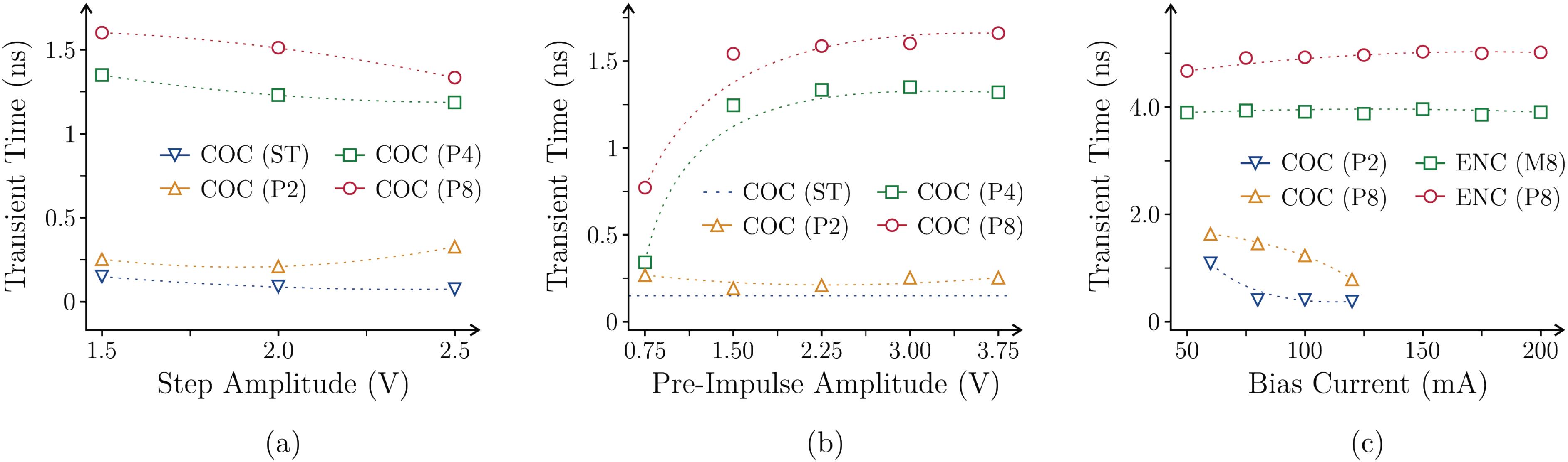
C. Transient Time
The transient time is measured as the time required for the switch to stabilize in its on-state (adopting as reference thresholds for variations smaller and bigger than 10 % of its stable level), being fundamental to evaluate the switch capability to transmit an optical signal without significant amplitude distortions. The most significant results are presented in Fig. 5, where the SOA bias currents, switching step amplitudes, and PISIC pre-impulse amplitudes cover all SOA operational conditions. Figure 5(a) shows that the switching step amplitude has little impact in the pulse overall stabilization. However, as expected, the injection of higher quantities of electrical carriers in wider pre-impulses (i.e., in the PISIC-4 and PISIC-8 cases) will lead to a more unstable rising transition. This behavior is also shown by the pre-impulse amplitude influence presented in Fig. 5(b), which, once more, advocates for the employment of the PISIC-2 technique in detriment of PISIC-4 and PISIC-8. The comparative analysis of Fig. 5(c) demonstrates, again, the advantages resulting from the parasitic reduction in the proposed microwave mounting, evidencing the transient time decreasing to less than half to the one achieved by the ENC-SOA. The smallest damping factor, which resulted in drastic overshoots, prevented successive oscillations after the overshoot induced by the PISIC preimpulse. Therefore, the SOA transient behavior stabilized in its on-state quicker, reducing the switch guard-time to less than 1 ns when employing the PISIC-2.
Experimental transient time analysis as a function of the SOA bias current, step amplitude, and impulse amplitude for the SOA COC-SOA (referred as COC) switched according to the STEP (ST) and PISIC techniques, this last one with preimpulses of 160 ps (P2), 320 ps (P4), and 640 ps (P8). Results for the SOA ENC-SOA (referred as ENC) switched with the PISIC and MISIC techniques, both with 640 ps pre-impulses (P8 and M8, respectively), are also presented as reference for the COC-SOA performance analysis. (a) COC-SOA switched with 80 mA bias and 3 V (60 mA) pre-impulses (except for the STEP technique); (b) COC-SOA switched with 80 mA bias and 1.5 V (30 mA) steps (STEP result presented as reference); (c) COC-SOA switched with 2.5 V (50 mA) steps and 3.75 V (75 mA) impulses and for the ENC-SOA with 2.5 V (50 mA) steps and 3 V (60 mA) impulses.
IV. Conclusion
A novel microwave mounting for SOA-based electro-optical switches, firstly proposed in [1212. [12] R. C. Figueiredo, T. Sutili, N. S. Ribeiro, C. M. Gallep, E. Conforti, “Semiconductor optical amplifier space switch with symmetrical thin-film resistive current injection,” IEEE/OSA Journal of Lightwave Technology, vol. 35, no.2, pp. 280-287, 2017. doi:10.1109/JLT.2016.2635202
https://doi.org/10.1109/JLT.2016.2635202...
], was experimentally characterized and analyzed comparatively with its encapsulated commercial counterpart. The results showed the importance of electrical parasitic reduction by the introduction of a microwave coupler constructed with a distributed thin-film resistor. The switch mounting, under the right operating conditions, was able to simultaneously reduces its rise time, percentage overshoot, and transient time. The achieved performance enables the device to operate in optical networks requiring ultra-high commutation rates space switches.
ACKNOWLEDGMENT
The authors wish to acknowledge the partial support of Brazilian agencies São Paulo Research Foundation (FAPESP - grants 2017/20121-8, 2015/50063-4, 2015/24517-8, and 2007/56024-4) and National Council for Scientific and Technological Development (CNPq - grants 301409/2017-0 and 402923/2016-2). The authors also thank M.Sc. Bruno Taglietti for his contribution obtaining the experimental results related to the encapsulated device employed as reference in this work.
REFERENCES
-
1.[1] A. Yi, L. Yan, Y. Pan, L. Jiang, Z. Chen, W. Pan, B. Luo, “Transmission of multi-dimensional signals for next generation optical communication systems,” Optics Communications vol. 408, pp. 42 – 52, 2018. doi:10.1016/j.optcom.2017.07.046.
» https://doi.org/10.1016/j.optcom.2017.07.046 -
2.[2] G. Chen, H. Guo, D. Zhang, J. Wu, X. Cao, N. Yoshikane, T. Tsuritani, I. Morita, “User-access-frequency statistics based hotspot adjustment in all-optically interconnected metro-embedded datacenters,” Optics Communications, vol. 381, pp. 437 – 442, 2016. doi:10.1016/j.optcom.2016.07.018.
» https://doi.org/10.1016/j.optcom.2016.07.018 -
3.[3] Y. Hong, X. Hong, J. Chen, S. He, “Elastic all-optical multi-hop interconnection in data centers with adaptive spectrum allocation,” Optics Communications, vol. 383, pp. 478-484, 2017. doi:10.1016/j.optcom.2016.09.027.
» https://doi.org/10.1016/j.optcom.2016.09.027 -
4.[4] P. Sharma, P. Pegus II, D. Irwin, P. Shenoy, J. Goodhue, J. Culbert, “Design and operational analysis of a green data center,” IEEE Internet Computing, vol. 21, no. 4, pp.16-24, 2017. doi:10.1109/MIC.2017.2911421.
» https://doi.org/10.1109/MIC.2017.2911421 -
5.[5] J. Yuan, D. Zhao, K. Long, Y. Zheng, “Improved immunization strategy to reduce energy consumption on nodes traffic,” Optics Communications, vol. 389, pp. 314 – 317, 2017. doi:10.1016/j.optcom.2016.12.045.
» https://doi.org/10.1016/j.optcom.2016.12.045 -
6.[6] T. Zhou, H. Jia, “Method to optimize optical switch topology for photonic network-on-chip,” Optics Communications, vol. 413, pp. 230 – 235, 2018. doi:10.1016/j.optcom.2017.12.062.
» https://doi.org/10.1016/j.optcom.2017.12.062 -
7.[7] A. E. Willner, S. Khaleghi, M. R. Chitgarha, O. F. Yilmaz, “All-optical signal processing,” IEEE/OSA Journal of Lightwave Technology, vol.32, no. 4, pp. 660-680, 2014. doi:10.1109/JLT.2013.2287219.
» https://doi.org/10.1109/JLT.2013.2287219 -
8.[8] X. Bana, X. Pang, X. Li, B. Hu, Y. Guo, H. Zheng, “A nonlinear plasmonic waveguide based all-optical bidirectional switching,” Optics Communications, vol. 406, pp. 124 – 127, 2018, doi: 10.1016/j.optcom.2017.06.040.
» https://doi.org/10.1016/j.optcom.2017.06.040 -
9.[9] G. Berrettini, A. Simi, A. Malacarne, A. Bogoni, L. Poti, “Ultrafast integrable and reconfigurable XNOR, AND, NOR, and NOT photonic logic gate,” IEEE Photonics Technology Letters, vol.18, no.8, pp. 917-919, 2006. doi: 10.1109/LPT.2006.873570.
» https://doi.org/10.1109/LPT.2006.873570 -
10.[10] Q. Guo, A. V. Tran, “Demonstration of 40-Gb/s WDM-PON system using SOA-REAM and equalization,” IEEE Photonics Technology Letters, vol.24, no.11, pp. 951-953, 2012. doi:10.1109/LPT.2012.2190051.
» https://doi.org/10.1109/LPT.2012.2190051 -
11.[11] C. Caillaud, P. Chanclou, F. Blache, P. Angelini, B. Duval, P. Charbonnier, D. Lanteri, G. Glastre, M. Achouche, “Integrated SOA-PIN detector for high-speed short reach applications,” IEEE/OSA Journal of Lightwave Technology, vol.33, no.8, pp. 1596-1601, 2015. doi:10.1109/JLT.2015.2389533.
» https://doi.org/10.1109/JLT.2015.2389533 -
12.[12] R. C. Figueiredo, T. Sutili, N. S. Ribeiro, C. M. Gallep, E. Conforti, “Semiconductor optical amplifier space switch with symmetrical thin-film resistive current injection,” IEEE/OSA Journal of Lightwave Technology, vol. 35, no.2, pp. 280-287, 2017. doi:10.1109/JLT.2016.2635202
» https://doi.org/10.1109/JLT.2016.2635202 -
13.[13] C. M. Gallep, E. Conforti, “Reduction of semiconductor optical amplifier switching times by pre-impulse step-injected current technique,” IEEE Photonics Technology Letters, vol. 14, no. 7, pp. 902-904, 2002. doi:10.1109/LPT.2002.1012379
» https://doi.org/10.1109/LPT.2002.1012379 -
14.[14] R. C. Figueiredo, N. S. Ribeiro, A. M. O. Ribeiro, C. M. Gallep, E. Conforti, “Hundred-picoseconds electro-optical switching with semiconductor optical amplifiers using multi-impulse step injection current,” IEEE/OSA Journal of Lightwave Technology, vol.33, no.1, pp. 69-77, 2015. doi:10.1109/JLT.2014.2372893
» https://doi.org/10.1109/JLT.2014.2372893 -
15.[15] J. Renaudier, A. C. Meseguer, A. Ghazisaeidi, P. Tran, R. R. Muller, R. Brenot, A. Verdier, F. Blache, K. Mekhazni, B. Duval, H. Debregeas, M. Achouche, A. Boutin, F. Morin, L. Letteron, N. Fontaine, Y. Frignac, G. Charlet, “First 100-nm continuous-band WDM transmission system with 115Tb/s transport over 100km using novel ultra-wideband semiconductor optical amplifiers,” in: 43rd European Conference on Optical Communication, vol. 1, 2017.
-
16.[16] P. Vorreau, A. Marculescu, J. Wang, G. Bottger, B. Sartorius, C. Bornholdt, J. Slovak, M. Schlak, C. Schmidt, S. Tsadka, W. Freude, J. Leuthold, “Cascadability and regenerative properties of SOA all-optical DPSK wavelength converters,” IEEE Photonics Technology Letters, vol.18, no.18, pp. 1970-1972, 2006. doi:10.1109/LPT.2006.880714.
» https://doi.org/10.1109/LPT.2006.880714 -
17.[17] T. Durhuus, B. Mikkelsen, C. Joergensen, S. L. Danielsen, K. E. Stubkjaer, “All-optical wavelength conversion by semiconductor optical amplifiers,” IEEE/OSA Journal of Lightwave Technology, vol.14, no.6, pp. 942-954, 1996. doi: 10.1109/50.511594.
» https://doi.org/10.1109/50.511594 -
18.[18] X. Zheng, O. Raz, N. Calabretta, D. Zhao, R. Lu, Y. Liu, “Multiport InP monolithically integrated all-optical wavelength router,” OSA Optics Letters, vol. 41, no. 16, pp. 3892-3895, 2016. doi:10.1364/OL.41.003892.
» https://doi.org/10.1364/OL.41.003892 -
19.[19] R. Farhat, A. Farhat, M. Menif, “Performances of two contention resolution units in optical SOA-MZI router,” Optics Communications, vol. 423, pp. 21 – 28, 2018. doi:10.1016/j.optcom.2018.04.002.
» https://doi.org/10.1016/j.optcom.2018.04.002 -
20.[20] A. Kotb, K. E. Zoiros, “Performance analysis of all-optical XOR gate with photonic crystal semiconductor optical amplifier-assisted Mach-Zehnder interferometer at 160 Gb/s,” Optics Communications, vol. 402, pp. 511-517, 2017. doi:10.1016/j.optcom.2017.06.050.
» https://doi.org/10.1016/j.optcom.2017.06.050 -
21.[21] M. Sahafi, A. Rostami, A. Sahafi, “All-optical high speed logic gates using SOA,” Optics Communications, vol. 285, no. 9, pp. 2289 – 2292, 2012. doi:10.1016/j.optcom.2012.01.018.
» https://doi.org/10.1016/j.optcom.2012.01.018 -
22.[22] R. C. Figueiredo, N. S. Ribeiro, C. de Mello Gallep, E. Conforti, “Frequency and time-domain simulations of semiconductor optical amplifiers using equivalent circuit modeling,” Optical Engineering, vol. 54, no. 11, 114107, 2015. doi:10.1117/1.OE.54.11.114107.
» https://doi.org/10.1117/1.OE.54.11.114107 -
23.[23] P. Rocha, C. M. Gallep, T. Sutili, E. Conforti, “Calibration of TLM Model for Semiconductor Optical Amplifier by Heuristic Parameters’ Extraction,” Journal of Microwaves, Optoelectronics and Electromagnetic Applications, vol. 17, no. 2, pp. 260-267, 2018. doi: 10.1590/2179-10742018v17i21208
» https://doi.org/10.1590/2179-10742018v17i21208 -
24.[24] T. Sutili, B. Taglietti, R. C. Figueiredo, C. D. M. Gallep, E. Conforti, “Guard time requirements for SOA-based electrooptical space switches and AM signals,” in: SBMO/IEEE MTT-S IMOC, Águas de Lindóia, Brazil, 2017. doi:10.1109/IMOC.2017.8121018.
» https://doi.org/10.1109/IMOC.2017.8121018
Publication Dates
-
Publication in this collection
Dec 2018
History
-
Received
12 June 2018 -
Reviewed
12 June 2018 -
Accepted
17 Sept 2018