Abstract
This work proposes the application of a slot in the ground plane, Defected Ground Structure (DGS), of a microstrip patch antenna. The application of this technique aims to attenuate higher-order excited modes without deteriorating the antenna parameters in the fundamental mode. The methodology for the design of the slot in H-format is presented, based on the physical dimensions of the microstrip patch antenna. The positioning of the DGS concerning the feed line was determined from a detailed parametric analysis. The antenna was designed for the fundamental mode at 2.45 GHz frequency. Two antenna prototypes were built, with and without DGS, and measurements of reflection coefficient, gain, and radiation pattern were performed. The measured results show that the application of DGS considerably attenuated higher-order excited modes. A good agreement between simulated and measured results is achieved.
Index Terms
DGS; Microstrip Antenna; Higher order suppression
I. INTRODUCTION
In recent years, there has been a great demand for mobile services and applications. Because of this, the use of wireless devices has increased significantly. In this type of device, the antenna plays a fundamental role. Through it, the device emits and receives electromagnetic signals at the desired frequency.
In this scenario, microstrip patch antennas present desirable characteristics for wireless communication devices. Due to reduced dimensions of most of these devices, these antennas are very attractive because they have attributes such as low profile, simple manufacturing, relatively low cost, easy adaptation to flat and non-flat surfaces, and easy integration with electronic circuits.
However, this type of antenna can radiate unwanted higher-order modes. These radiated modes may contribute to an increase in levels of electromagnetic interference [1[1] L. Borwn et al., “Harmonic suppression with photonic bandgap and defected ground structure for a microstrip patch antenna,” IEEE Microwave and Wireless Components Letters, vol. 15, no. 2, pp. 55–56, 2005.], [2[2] M. H. Chang et al., “Microstrip-fed ring slot antenna design with wideband harmonic suppression,” IEEE Transactions on Antennas and Propagation, vol. 62, no. 9, pp 4828–4832, 2014.]. To reduce these levels of interference, wireless devices may have to incorporate filters, preventing signals outside the desired frequency from being emitted or received [2[2] M. H. Chang et al., “Microstrip-fed ring slot antenna design with wideband harmonic suppression,” IEEE Transactions on Antennas and Propagation, vol. 62, no. 9, pp 4828–4832, 2014.], [3[3] Y. J. Sung, M. Kim, and Y. S. Kim, “Harmonics reduction with defected ground structure for a microstrip patch antenna,” IEEE Antennas and Wireless Propagation Letters, vol. 2, pp 111–113, 2003.]. Applying filters can contribute to other issues such as increasing the size, weight, and cost of the wireless device. In this way, some alternative solutions that do not increase cost or complexity for the device can be attractive. Thus, solutions that use the antenna itself to filter these higher-order modes become interesting [4[4] S. Biswas, D. Guha, and C. Kumar, “Control of higher harmonics and their radiations in microstrip antennas using compact defected ground structures,” IEEE Transactions on Antennas and Propagation, vol. 61, no. 6, pp 3349–3353, 2013.], [5[5] U. Pattapu, S. P. Biswal, and S. Das, “A 2.45 GHz DGS based harmonic rejection antenna for rectenna application,” Proc. 2017 USNC-URSI Radio Science Meeting, July, pp 123–124, 2017.].
Several studies are being developed for design designing antennas able to attenuate or suppress unwanted frequencies. Among the techniques used, we can highlight the use of periodic structures and DGS insertion. Periodic structures can increase the complexity and fabrication cost of the antenna, reducing some advantages of this antenna type, whereas the DGS generally uses simple geometries and is capable of providing rejection in a wide bandwidth [6[6] Y. J. Sung, C. S. Ahn, and Y. S. Kim, “Size reduction and harmonic suppression of rat-race hybrid coupler using defected ground structure,” IEEE Microwave and Wireless Components Letters, vol. 14, no. 1, pp 7–9, 2004.], [7[7] F. C. B. Sena and J. P. Silva, “Harmonic suppression using optimised hexagonal defected ground structure by genetic algorithm,” IET Microwaves, Antennas & Propagation, vol. 12, no. 10, pp 1645–1648, 2018.].
This work proposes the use of DGS in H-format for attenuation of higher-order excited modes in a microstrip patch antenna for WLAN application. The reference antenna radiates higher-order modes over a frequency range of 3 GHz to 10 GHz, which can cause interference in systems using licensed frequencies. The idea is to attenuate as much as possible all higher-order modes within this frequency range of interest. The methodology, discussions, and results will be demonstrated in the following sessions.
II. Previous Works
In [2[2] M. H. Chang et al., “Microstrip-fed ring slot antenna design with wideband harmonic suppression,” IEEE Transactions on Antennas and Propagation, vol. 62, no. 9, pp 4828–4832, 2014.], Chang et al. proposed a circular patch antenna for WLAN application at the fundamental frequency of 2.45 GHz. To suppress the higher-order harmonic modes a ring DGS combined with an inverted U-shaped DGS were incorporated into the project. The technique allowed the suppression of up to 4 higher-order modes. The proposed antenna maintained the performance parameters of the original antenna, such as radiation pattern and gain.
Biswas et al. [4[4] S. Biswas, D. Guha, and C. Kumar, “Control of higher harmonics and their radiations in microstrip antennas using compact defected ground structures,” IEEE Transactions on Antennas and Propagation, vol. 61, no. 6, pp 3349–3353, 2013.] investigated harmonic suppression in rectangular patch antenna for S-band application around 3.11 GHz, using a stub, to improve impedance matching. Harmonic suppression was achieved by the addition of two truncated circular rings aligned with the microstrip feed line. The project allowed the suppression of 6 higher-order modes. However, the final set had a relatively large occupied area, which may be inappropriate for some applications.
Pattapu et al. [5[5] U. Pattapu, S. P. Biswal, and S. Das, “A 2.45 GHz DGS based harmonic rejection antenna for rectenna application,” Proc. 2017 USNC-URSI Radio Science Meeting, July, pp 123–124, 2017.] proposed a circular patch antenna applied for power transmission. The design operating frequency was 2.45 GHz. It was proposed to insert two DGS on a ground plane, one was a rectangular DGS and the other one was a loop DGS for suppression of higher-order harmonics. The results show a good attenuation in the rejection range, but the area occupied on the ground plane was relatively large. This situation decreased the total gain, as well as the front-to-back ratio.
Sena et al. [7[7] F. C. B. Sena and J. P. Silva, “Harmonic suppression using optimised hexagonal defected ground structure by genetic algorithm,” IET Microwaves, Antennas & Propagation, vol. 12, no. 10, pp 1645–1648, 2018.] proposed the use of genetic algorithms to optimize the design of hexagonal slots to suppress higher-order modes. The antenna was designed for 5.8 GHz. An optimization using AG was performed to adjust the number and diameter of the slots, distance between it and positions in the ground plane. The proposal allowed the attenuation of a relatively small number of higher-order modes, as well as causing an increase in back radiation, reducing gain and efficiency.
Rahim et al. [8[8] A. Rahim et al., “A Harmonic Suppression Circular Disk Microstrip Patch Antenna at the 2.45 GHz Frequency,” Proc. 2014 IEEE Colloquium on Humanities, Science & Engineering Research, April, pp 1–5, 2014.] proposed a circular patch antenna for the frequency of 2.45 GHz. For suppression of higher-order harmonics, the authors inserted 5 non-uniform rectangular slots as DGS. In addition, to improve impedance matching, the authors inserted a stub in a microstrip feed line. The proposal modifications allowed an improvement in impedance matching, but the attenuation of higher-order modes was limited. In addition, the authors made no comparison with the performance parameters between the reference antenna and the proposed antenna.
In [9[9] P. R. Prajapati, “Application of defected ground structure to suppress out-of-band harmonics for WLAN microstrip antenna,” International Journal of Microwave Science and Technology, pp 1–9, 2015.], the authors proposed a rectangular patch microstrip antenna that incorporates fractal slots at 2.45 GHz with coupling feed. For attenuation of higher-order modes, an H-format DGS was added below the power line. The authors note that the variety of techniques has added improvements to impedance matching, radiation efficiency, and size reduction. However, the proposed antenna is complex and the performance is below when compared to other antennas presented in the state of the art of this work.
In [10[10] J. Acharjee et al., “Suppressing up to fourth harmonic of an ISM band microstrip patch antenna using compact defected ground structures,” Microwave and Optical Technology Letters, vol. 59, no. 9, pp 2254–2259, 2017.], the authors proposed a rectangular patch antenna to operate at 2.45 GHz. To improve the impedance matching a L-shaped stub was added to the microstrip feed line. For suppression of higher-order harmonics, two I-format DGS were added under the microstrip feed line. The proposal allowed the suppression of a significant number of higher-order modes. However, the DGS occupied a significant area which led to a reduction in performance parameters such as gain and radiation diagram.
In this work, we propose a rectangular microstrip patch antenna, to operate at 2.45 GHz. For higher-order modes suppression, we propose to insert an H-shaped DGS. We used the equivalent circuit to design the initial dimensions of DGS. Besides, to improve impedance matching we use the ANSYS HFSS optimization tool, to indicate the best position of DGS concerning the inset fed. Thus, our proposal achieves significant higher-order mode suppression without causing changes in antenna performance parameters due to the minimum ground area occupancy. The performances of cited works in this section are compared in TABLE I. The results are compared in terms of the fundamental frequency, the number of higher-order modes suppressed, the proposed technique, and the area occupied by the DGS.
III. Antenna Design
Initially, a microstrip patch antenna was designed to be used in the WLAN frequency, at 2.45 GHz. The dielectric considered in the design was the FR4, with a thickness of 1.6 mm, an electrical permittivity of 4.4 and a loss tangent of 0.02. Fig. 1 illustrates the physical characteristics of the reference patch antenna, which is designed to operate in the dominant mode (TM10) at 2.45 GHz.
The antenna design follows the classic approach in [11[11] C. A. Balanis, Antenna Theory: Analysis and Design, NY, USA, John Wiley & Sons, 2005.]. To obtain an input impedance of 50Ω, the length and width of the feed line were calculated appropriately. To achieve an effective impedance matching, the inset-fed technique was used. The feed line width value (Wf) is related to the thickness (h) and effective dielectric constant (εef) of the substrate. The inset-fed (Y0) of the line is related to input resistance (Rin) and patch length [11[11] C. A. Balanis, Antenna Theory: Analysis and Design, NY, USA, John Wiley & Sons, 2005.], [12[12] D. M. Pozar, Microwave Engineering, NY, USA, John Wiley & Sons, 2011.]. TABLE II summarizes the values obtained after the design calculations.
After the design, these specifications were considered for modeling and simulation within the ANSYS HFSS software. Simulations were performed for reflection coefficient, gain, radiation pattern and Smith chart. Fig. 2 shows the frequency response of |S11| in dB. It can be observed that in addition to the fundamental mode (TM10) the antenna radiates TM20, TM30 and TM40 harmonic modes (2nd, 3rd, and 4th harmonics, respectively), TM02 and TM22 higher-order modes, and two spurious modes.
The excited modes are analyzed by the electric field distribution on the patch antenna. According to [11[11] C. A. Balanis, Antenna Theory: Analysis and Design, NY, USA, John Wiley & Sons, 2005.], to determine the resonant modes, TMmn, we must evaluate the number of variations maximum and minimum of the electric field potential. Thus, the evaluation of the modes is given by the analysis of the electric field distribution on the radiating patch element regarding Lp (length) and Wp (width). The modes are excited at a given resonant frequency, fmn, where m and n represent the number of potential variations along with Lp and Wp of the antenna patch. In this way, it is possible to determine the resonant mode for the frequency range of interest.
The fundamental (dominant) mode, represented by TM10 represents the lowest frequency of the range of interest. The other modes are considered high order excited modes which, for this study, are not desired. From (1), it is possible to calculate the resonance frequency for a given mode [11[11] C. A. Balanis, Antenna Theory: Analysis and Design, NY, USA, John Wiley & Sons, 2005.]:
where c is the light speed in free space and εr is the relative permittivity of the substrate.
The following investigations are intended to examine the radiated electric fields for the modes. It is possible to identify higher-order modes through the study of modal fields. It can be observed the excited modes of the reference antenna in Fig. 3. So, modes: TM20, TM30 and TM40 are the 2nd, 3rd and 4th harmonics of the fundamental mode frequency. Other modes are presented but are not characterized as harmonic modes. Spurious modes arise from the approximation of harmonic modes. In the case of microstrip antennas, spurious modes are also excited by surface waves. It was not the object of study in this work. The excited modes have the characteristic of concentrating the electric field in the patch of the antenna, mainly in its extremities. In Fig. 3, the region in darker red represents a greater concentration of electric field, while the region in darker blue represents a lower concentration.
Simulated electric field in the patch: (a) TM10 (fundamental), (b) TM02, (c) spurious, (d) TM20, (e) TM22, (f) TM30, (g) spurious, and (h) TM40.
Fig. 4 shows the electric field distribution and current flow in the ground plane and patch element, for the fundamental mode. A concentration of the electric field at the ends of the ground plane of the antenna is observed while the current distribution is concentrated below the patch area to the center.
Distribution in the ground plane of the antenna without DGS: (a) electric field and (b) current.
IV. DGS Design
Fig. 5 (a) illustrates the proposed DGS section, which is located on the ground plane. The DGS behaves like a low-pass single-pole filter that has a cut-off frequency and an attenuation pole [13[13] A. K. Arya, M. V. Kartikeyan, and A. Patnaik, “Defected ground structure in the perspective of microstrip antennas: a review,” Frequenz, vol. 64, no. 5, pp 79–84, 2010.] – [18[18] A. Boutejdar et al., “An Improvement of Defected Ground Structure Lowpass/Bandpass Filters Using H-Slot Resonators and Coupling Matrix Method,” Journal of Microwaves, Optoelectronics and Electromagnetic Applications, vol. 10, no. 2, pp 295–307, 2011.]. The cut-off frequency (fc) is dependent to the area of the DGS occupied on the ground plane. The attenuation pole (f0), on the other hand, depends on the position in which the DGS is impressed in the ground plane [13[13] A. K. Arya, M. V. Kartikeyan, and A. Patnaik, “Defected ground structure in the perspective of microstrip antennas: a review,” Frequenz, vol. 64, no. 5, pp 79–84, 2010.] – [18[18] A. Boutejdar et al., “An Improvement of Defected Ground Structure Lowpass/Bandpass Filters Using H-Slot Resonators and Coupling Matrix Method,” Journal of Microwaves, Optoelectronics and Electromagnetic Applications, vol. 10, no. 2, pp 295–307, 2011.]. Both still depend on the combination of inductance and capacitance elements. Fig. 5 (b) illustrates the equivalent circuit representing the DGS. The impedances Z0 are from the generator and antenna. The effects of inductance and capacitance can be added or mitigated by the dimensions of the DGS. The cut-off frequency is inversely proportional to the physical dimensions of the vertical arms of H. The physical dimensions of the connecting bar between the vertical arms of H will cause the rejection bandwidth to be higher.
The vertical arms of H are dimensioned by Lh and Wh, and the connection bar, dimensioned by Wb and Lb. The DGS H-format allows easy and predictable adjustments to the electrical parameters (RLC) through their dimensions. Adjustments are done based on four parameters: the length and width of the weights (arms) and the length and width of the connection bar between the weights. Through these, adjustments become possible that will allow allocating the rejection band as desired.
The analysis and design part of the DGS were presented in [10[10] J. Acharjee et al., “Suppressing up to fourth harmonic of an ISM band microstrip patch antenna using compact defected ground structures,” Microwave and Optical Technology Letters, vol. 59, no. 9, pp 2254–2259, 2017.], [18[18] A. Boutejdar et al., “An Improvement of Defected Ground Structure Lowpass/Bandpass Filters Using H-Slot Resonators and Coupling Matrix Method,” Journal of Microwaves, Optoelectronics and Electromagnetic Applications, vol. 10, no. 2, pp 295–307, 2011.]. Our design should allow suppression of higher-order modes while maintaining the S11 greater than – 8 dB for all modes but without affecting antenna performance. The intention is, if possible, to improve some performance parameters. Thus, we designed the DGS to have a cut-off frequency equal to twice the antenna frequency (4.9 GHz) and a rejection bandwidth sufficient to suppress higher-order modes, of a resonance frequency of 9 GHz. To find the optimal position of the DGS in the ground plane the ANSYS HFSS optimization tool was used. Thus, this position allowed the best antenna impedance matching, occupying the smallest possible area, maintaining important characteristics such as front-to-back ratio, gain, and unchanged radiation diagram. The projected dimensions are listed in TABLE III.
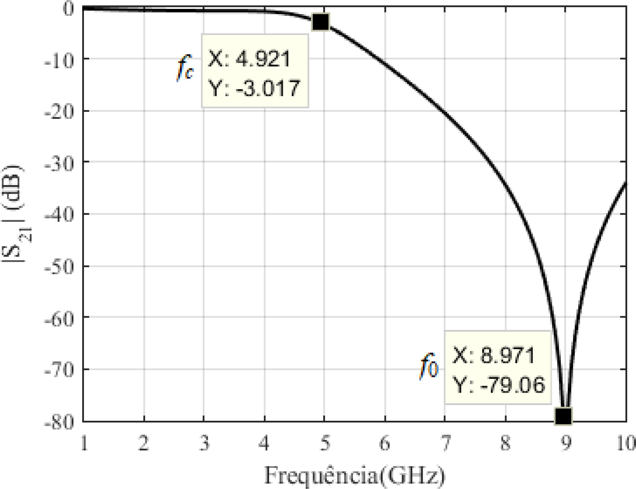
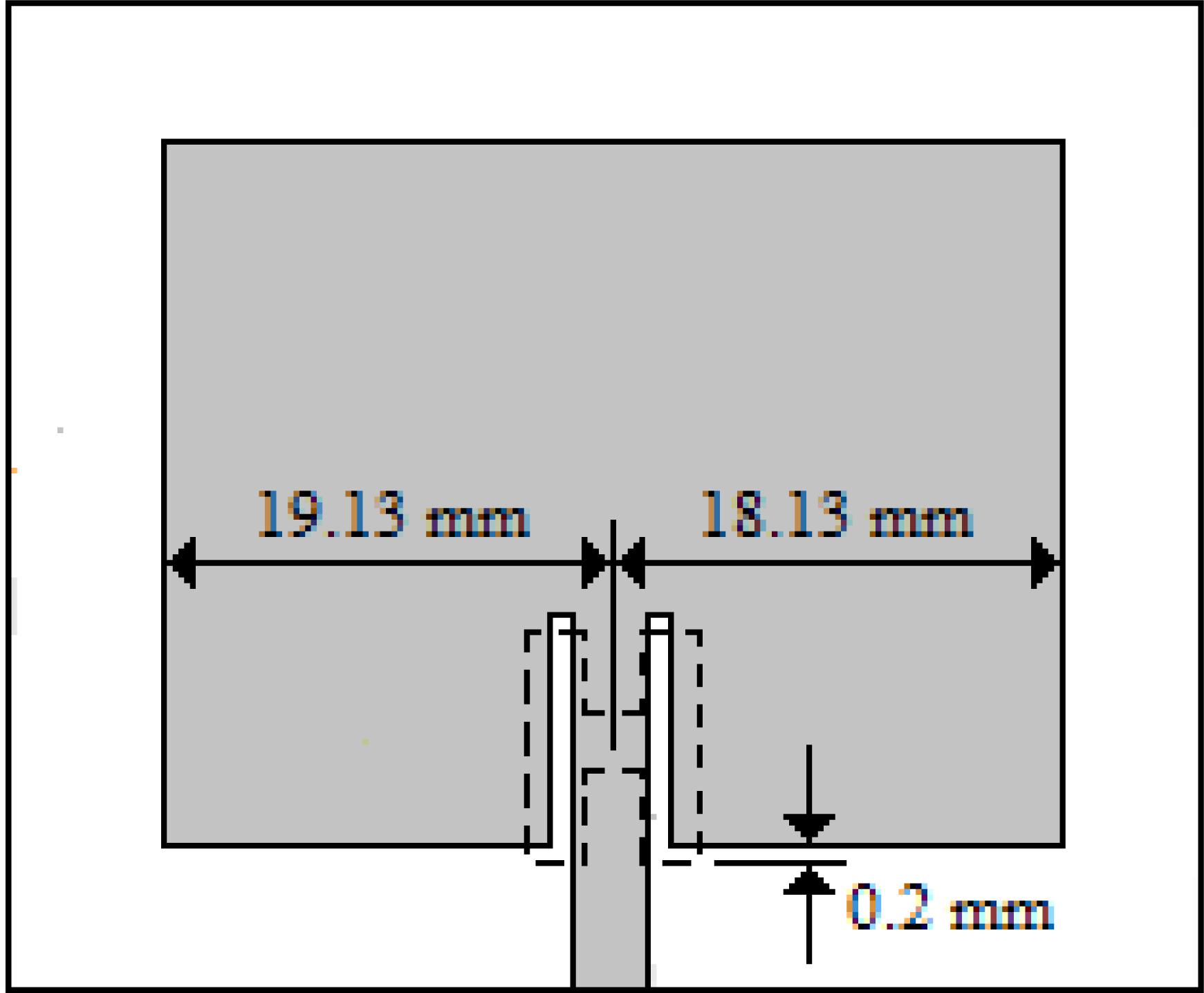
To investigate the frequency characteristics of DGS, it was simulated the same in the ANSYS HFSS. The simulation results show that the cut-off frequency and attenuation pole, as well as bandwidth characteristics, converged as expected. Fig. 6 illustrates the frequency response of DGS S21. The cut-off frequency, fc, was 4.921 GHz and resonance frequency, f0, was 8.971 GHz. Although the first three resonant modes, TM02 (3.84 GHz), spurious (4.65 GHz), and TM20 (4.83 GHz) are close to the cut-off frequency, the optimization of the DGS positioning allowed the suppression of these modes. After parameterization using the ANSYS HFSS optimization tool, the DGS was positioned on the ground plane as shown in Fig. 7. In our case, the DGS was not centralized concerning the feed line. It was displaced from 1.0 mm relative to the center of the feed line to the right and 0.2 mm in direction of the lower edge of the patch.
The reactive components shown in Fig. 5, C and L can be calculated as function of fc and f0 as [18[18] A. Boutejdar et al., “An Improvement of Defected Ground Structure Lowpass/Bandpass Filters Using H-Slot Resonators and Coupling Matrix Method,” Journal of Microwaves, Optoelectronics and Electromagnetic Applications, vol. 10, no. 2, pp 295–307, 2011.]:
where Z0 is the characteristic impedance of 50 Ω.
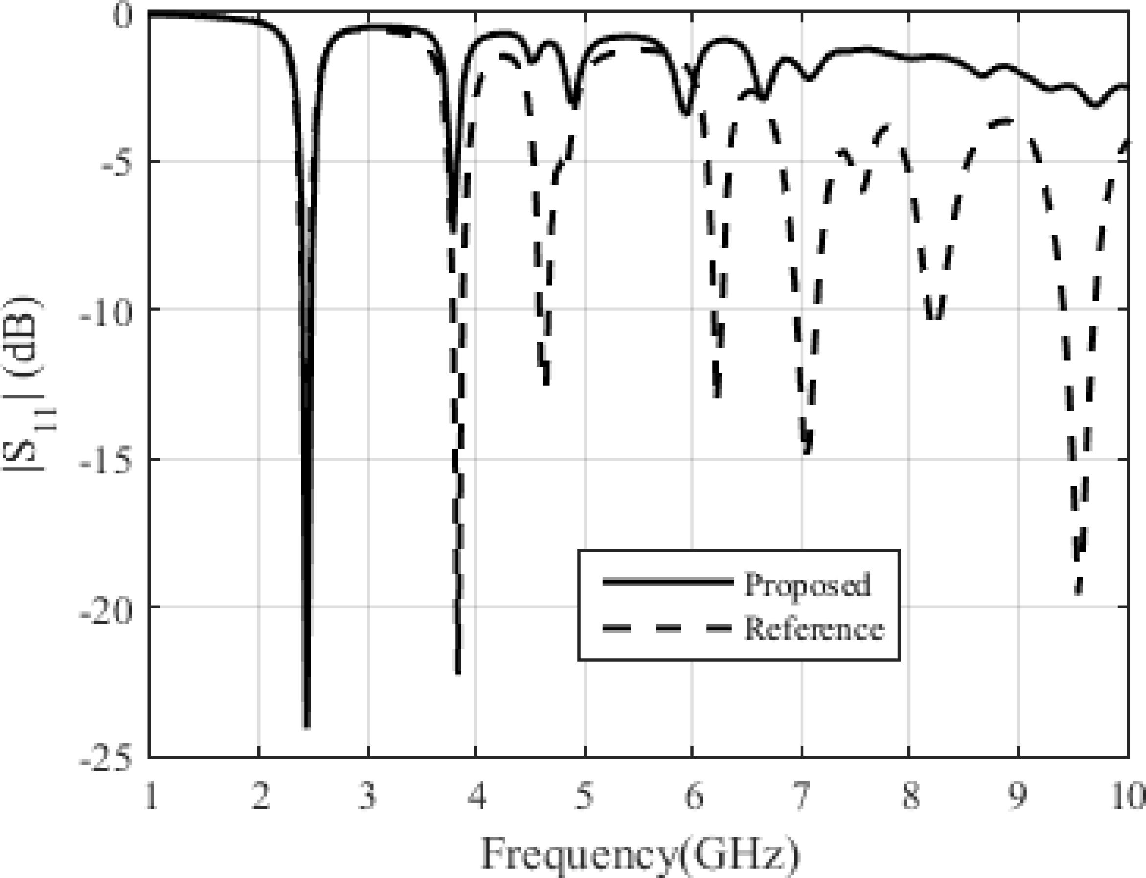
After the design and analysis of the DGS influence on fundamental mode, simulations were performed in order to obtain some parameters of the antenna. Fig. 8 shows a comparison between the S11 of the reference antenna and the proposed antenna. It can be observed that the proposed antenna presents better results, because besides completely suppressing most of the higher-order modes and, in the frequency range between 2.5 GHz to 10 GHz, also improved the impedance matching at 2.45 GHz, by reducing the S11 from – 20 dB to – 24 dB.
In fact, that occurs because the impedance of the reference antenna is 47.48 + j16.98 Ω and with the parametrization of the position of the DGS the impedance has a significant decrease of the reactive part and an increase of the resistive part. So, the proposed antenna obtains an impedance of 51.83 + j0.08 Ω.
Fig. 9 (a) illustrates the electric field distribution and Fig. 9 (b) illustrates the current flow in the proposed ground plane and patch antenna. With the insertion of the DGS, the electric field distribution changes and there is a concentration of it in the edges of the DGS. We can observe a small change in the flow of current.
Distribution in the ground plane of the antenna with DGS: (a) electric field and (b) current.
V. Measured Results
For purposes of proving the effects addressed in the previous sections, two prototypes were constructed, one of the reference antenna and the other of the proposed antenna. These prototypes are illustrated in Fig. 10.
Measurements were performed with an Agilent Technologies brand vector network analyzer: model E5071C with a measurement frequency range from 1 to 10 GHz, for visualization of higher-order modes, within this range of interest. Fig. 11 shows the measurement setup, where AUT is the antenna under test.
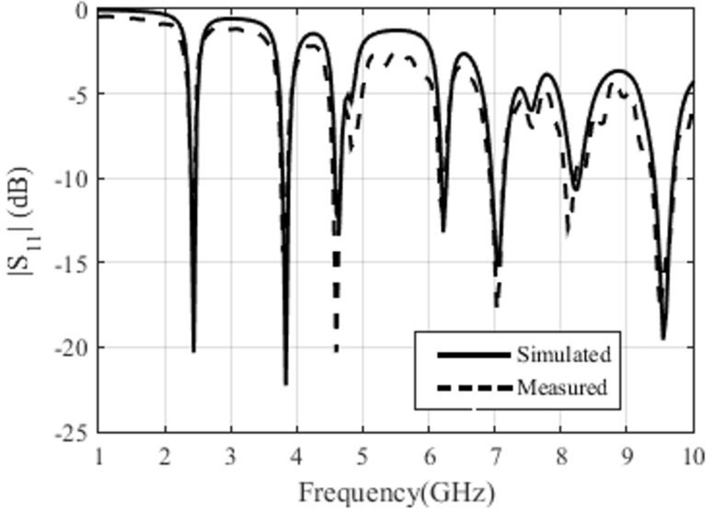
The first measurement was performed for the reference antenna. We measure the S11 to prove the existence of higher-order modes. Fig. 12 illustrates this measurement. It can be noticed that all modes confirmed in simulation appear. A good agreement between the results can be observed.
Then, measurements for the proposed antenna with the DGS in H-format were performed. As in simulation, the DGS altered the antenna impedance, significantly attenuating the higher modes, and most of them were suppressed. Once again, a good agreement between the results can be observed. Fig. 13 illustrates this proof.
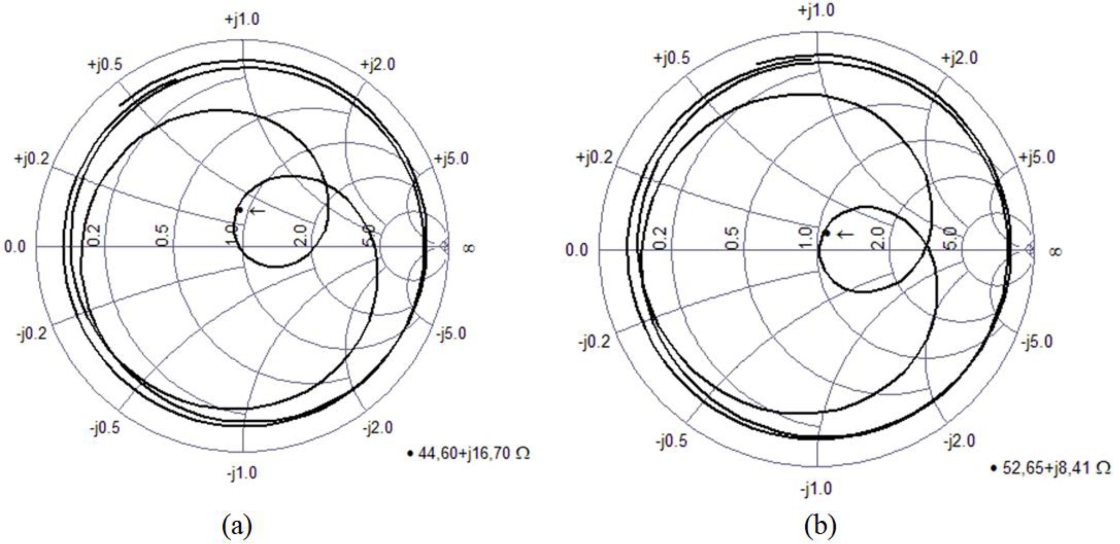
Fig. 14 (a) shows the measured Smith chart for the reference antenna. We can see that there is good agreement with the simulated results. As in the simulation, the inductive reactance is significant, with values closer to zero being desirable.
Comparison between (a) measured Smith chart for the reference antena and (b) measured Smith chart for the proposed antenna.
The measured Smith chart, for the proposed antenna, is shown in Fig. 14 (b). As for the simulated values, it can be seen that a significant reduction of the inductive reactive part of this parameter occurred, as well as, it can be observed that improvement in impedance matching.
Table 4 presents a comparison between results for the reference antenna and proposed antenna with DGS. It can be noticed that there was no parameter change for the frequency of interest (2.45 GHz). It is worth mentioning the good agreement between the simulated and measured values. In addition to improvements already highlighted for the proposed antenna, without adding constructive complexity.
The simulated co- and cross-polarized radiation patterns and measured co-polarized radiation pattern of the reference and proposed antenna on E-plane, at the resonant frequency 2.44 GHz are plotted in Fig. 15(a). It shows that the antenna has a directional radiation pattern in E-plane. The cross-polarization level is more than 40 dB below than the co-polarization level. Fig. 15(b) illustrates simulated co- and cross-polarized radiation patterns of the reference and proposed antenna on H-plane, at the resonant frequency 2.44 GHz. The cross-polarization level is more than 20 dB below than the co-polarization level. Results show that the reference and proposed antennas present almost the same radiation patterns, in both E- and H-plane.
Radiation pattern for reference and proposed antenna: (a) measured and simulated at E-plane and (b) simulated at H-plane.
VI. Conclusions
This work aimed on suppression of radiated higher-order modes. To this end, a DGS with H-format was added to the ground plane of the antenna. The DGS was designed to reduce the large inductive reactance of the reference antenna and its insertion produced a reduction of 50 % in that value. There was a suppression of almost all higher-order modes within the frequency range of interest, considering excitations below S11 of −10 dB. The antenna parameters at the frequency of interest, 2.45 GHz, remained unchanged, with an improvement of others. It was possible because we optimize the position of the DGS, using the ANSYS HFSS optimization tool. The proposed antenna preserved the frequency fundamentally and limited interference problems without the need to couple filters to the communication system. It is suitable for applications in compact and low-cost communication systems.
ACKNOWLEDGMENT
The authors thank the Postgraduate Program in Electrical and Computer Engineering (PPgEEC) of the Federal University of Rio Grande do Norte (UFRN), the Federal Institute of Education, Science and Technology of Paraiba (IFPB), the Federal Institute of Education, Science and Technology of Rio Grande do Norte (IFRN) and the Federal University of Campina Grande (UFCG), to support the construction of this work.
REFERENCES
-
[1]L. Borwn et al, “Harmonic suppression with photonic bandgap and defected ground structure for a microstrip patch antenna,” IEEE Microwave and Wireless Components Letters, vol. 15, no. 2, pp. 55–56, 2005.
-
[2]M. H. Chang et al, “Microstrip-fed ring slot antenna design with wideband harmonic suppression,” IEEE Transactions on Antennas and Propagation, vol. 62, no. 9, pp 4828–4832, 2014.
-
[3]Y. J. Sung, M. Kim, and Y. S. Kim, “Harmonics reduction with defected ground structure for a microstrip patch antenna,” IEEE Antennas and Wireless Propagation Letters, vol. 2, pp 111–113, 2003.
-
[4]S. Biswas, D. Guha, and C. Kumar, “Control of higher harmonics and their radiations in microstrip antennas using compact defected ground structures,” IEEE Transactions on Antennas and Propagation, vol. 61, no. 6, pp 3349–3353, 2013.
-
[5]U. Pattapu, S. P. Biswal, and S. Das, “A 2.45 GHz DGS based harmonic rejection antenna for rectenna application,” Proc. 2017 USNC-URSI Radio Science Meeting, July, pp 123–124, 2017.
-
[6]Y. J. Sung, C. S. Ahn, and Y. S. Kim, “Size reduction and harmonic suppression of rat-race hybrid coupler using defected ground structure,” IEEE Microwave and Wireless Components Letters, vol. 14, no. 1, pp 7–9, 2004.
-
[7]F. C. B. Sena and J. P. Silva, “Harmonic suppression using optimised hexagonal defected ground structure by genetic algorithm,” IET Microwaves, Antennas & Propagation, vol. 12, no. 10, pp 1645–1648, 2018.
-
[8]A. Rahim et al., “A Harmonic Suppression Circular Disk Microstrip Patch Antenna at the 2.45 GHz Frequency,” Proc. 2014 IEEE Colloquium on Humanities, Science & Engineering Research, April, pp 1–5, 2014.
-
[9]P. R. Prajapati, “Application of defected ground structure to suppress out-of-band harmonics for WLAN microstrip antenna,” International Journal of Microwave Science and Technology, pp 1–9, 2015.
-
[10]J. Acharjee et al, “Suppressing up to fourth harmonic of an ISM band microstrip patch antenna using compact defected ground structures,” Microwave and Optical Technology Letters, vol. 59, no. 9, pp 2254–2259, 2017.
-
[11]C. A. Balanis, Antenna Theory: Analysis and Design, NY, USA, John Wiley & Sons, 2005.
-
[12]D. M. Pozar, Microwave Engineering, NY, USA, John Wiley & Sons, 2011.
-
[13]A. K. Arya, M. V. Kartikeyan, and A. Patnaik, “Defected ground structure in the perspective of microstrip antennas: a review,” Frequenz, vol. 64, no. 5, pp 79–84, 2010.
-
[14]C. Garg, and M. Kaur, “A review of defected ground structure (DGS) in microwave design,” International Journal of Innovative Research in Electrical, Electronics, Instrumentation and Control Engineering, vol. 2, no. 3, pp 1285–1290, 2014.
-
[15]D. Ahn et al, “A Design of the Low-Pass Filter Using the Novel Microstrip Defected Ground Structure,” IEEE Transactions on Microwave Theory and Techniques, vol. 49, no. 1, pp 86–93, 2001.
-
[16]J. S. Lim et al., “Design of Lowpass Filters Using Defected Ground Structure and Compensated Microstrip Line,” Electronics Letters, vol. 38, no. 22, pp 1357–1358, 2002.
-
[17]C. S. Kim et al., “A Novel 1-D Periodic Defected Ground Structure for Planar Circuits,” IEEE Microwave and Guided Wave Letters, vol. 10, no. 4, pp 131–133, 2000.
-
[18]A. Boutejdar et al, “An Improvement of Defected Ground Structure Lowpass/Bandpass Filters Using H-Slot Resonators and Coupling Matrix Method,” Journal of Microwaves, Optoelectronics and Electromagnetic Applications, vol. 10, no. 2, pp 295–307, 2011.
Publication Dates
-
Publication in this collection
08 June 2020 -
Date of issue
June 2020
History
-
Received
20 Dec 2019 -
Reviewed
26 Dec 2019 -
Accepted
18 Apr 2020