 Advancements in Microlenses and their Diverse Applications in Optical Sensors
Abstract
The fabrication and characterization are two areas where the microlenses have been widely studied. The integration of microlenses into microdevices was the main slingshot to achieve the fabrication of compact optical microsystems with reduced sizes, low-cost and on a reproducible way. The main driver of cost reduction was the use of standard microfabrication techniques found on the microlectronics industry. The actual interest of microlenses is the light gathering/projection and focusing for optimizing the light acquisition/production and thus, to improve the sensitivity/efficiency of optical microsystems either working as sensor or as source. In this context, this paper makes a review of microlenses for application in optical sensors. This review describes fabrication technologies, characteristics and applications of microlenses. This review also gives special emphasis on a case study of polymeric microlenses obtained by thermal reflow and at the same time, it also demonstrates the feasibility to augment light into photodiodes.
Keywords:
Optical microsystem; microlenses; micro-fabrication; CMOS.
HIGHLIGHTS
Compact microlenses enhance optical microsystem efficiency.
Integration of microlenses through standard microfabrication techniques.
Improved sensitivity and light optimization in optical sensors.
Case study on polymeric microlenses for photodiode light augmentation.
INTRODUCTION
Lenses have been used for quite some time and, throughout their development history, their applications vary considerably. Lenses are passive optical devices that are used, generally, for refracting and transmitting light. For example, lenses were found to be very useful in applications from concentrating sunlight for producing fire, to spectacles for improving eye sight and on telescopes and microscopes for studying the cosmos and microorganisms [1], respectively. More recently, the so called microlenses are used for a number of applications in the micro/nanoscale small, whose diameters are smaller than one millimeter. Examples of applications of microlenses include imaging, biomedical instruments, lab on a chip system and a variety of uses in optical communications [2-11].
In order to understand the focus behind this paper and taking the specific case of an image sensor (imager), any one knows that the interest to use microlenses on an imager is to improve the gathering of light and it focusing into the photodetectors. All the major companies in the market of digital cameras offer several products containing microlenses for optimizing the acquisition of light. A digital camera with microlenses optimizes the way the light is collected, resulting in the quality improvement of the captured image.
More electron-holes pairs are generated with microlenses because more photons from the scene or the object are captured, hence improving the sensitivity and at the same time, obtaining more useful information for digital processing. In this particular example, the aim to increase the number of photons per unity of area is to compensate the reduction in the size of the pixels required to enhance the resolution. In this context, this paper presents a review of microlenses for application on optical microsystems, by describing the fabrication processes currently available, applications and finishing with a case study using polymeric microlenses obtained by photolithography, thermal reflow and rehydration.
LENSES
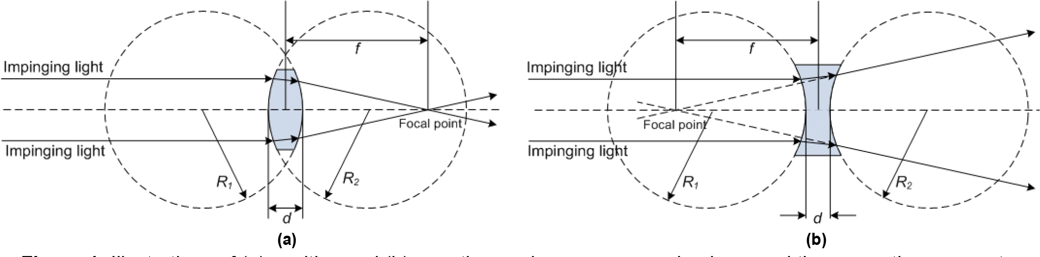
As illustrated in Figure 1, lenses are characterized by their curvature on both sides and are positive or negative when the surface is convex or concave towards the impinging light, respectively [12]. In the case of positive lenses, this means that when light crosses the lens, it will be converged into a single point located at a distance f, called focal point or focal length. In relation to the negative lenses, the incoming light is diverged when exiting the lens but it seems as it is originating from a point located on the front side of the lens, being also the focal length f but measured in negative units when compared to the f in positive lenses.
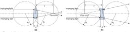
Illustrations of (a) positive and (b) negative equiconvex converging lens, and the respective parameters.
The effect that positive and negative lenses have on the light propagation path is also dependent on the Snell’s law given by n1.sin(θ1)=n2.sin(θ2) [13], where n1 and n2 are the indexes of refraction of two different materials (normally, the medium 1 is the air, while the medium 2 is the material of which the lens is made of, making n1<n2), θ1 and θ2 are the angles referenced to the surface normal of the incident and refracted (or transmitted) light, respectively. This equation represents the light deflection due to the refraction which happens when light encounters an interface between two materials with different indexes of refraction n. In this sequence, Figure 1 also illustrates the most important parameters concerning the design of positive and negative lenses. Figure 1(a) refers to a positive equiconvex converging lens, where the center is thicker than the edges meaning that the light converges more as it crosses the material with higher index of refraction than air. Figure 1(b) refers to a negative equiconvex converging lens, where the edges are thicker than the center meaning that the light diverges more as it crosses the material with higher index of refraction than air. Table 1 lists the main variations in both radius presented in the Figure 1, considering the different curvatures on both sides of a lens [14]. The lenses more suitable to integrate on microsystems are the plano-convex because are the easiest to fabricate and at same time are used in the majority of applications.
The first microlenses were fabricated for the first time in 1988 [15] and opened a large number of new applications. Nowadays, the microlenses are normally used on collimation and focusing. There are two important types of plano-convex microlenses: the spherical and the aspherical. The profile of a spheric lens is circular whereas the aspheric lens is not. This means that due to its particular profile, the aspheric lenses are difficult to fabricate with conventional, simple processes [14,16].
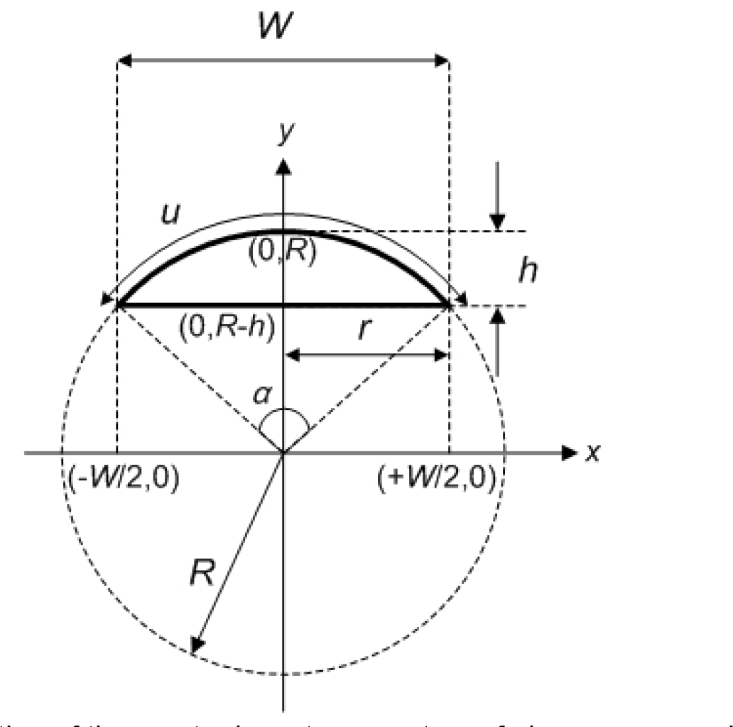
The spherical lenses are easier to fabricate than the aspherical but present aberration. Normally, this problem can be ignored in the majority of the applications without bringing significant negative effects. Aspheric lenses, unlike their counterparts, are able to focus all the parallel incoming rays of light into the same focal point. This focusing issue can be critical depending on the application. Therefore, lenses with spherical surfaces are the ones of interest in the context of this review, more specifically, plano-convex lenses. Nevertheless, a plano-convex lens is a particular case of general spherical lenses. The cross-section of a spherical lens is a circular segment, as illustrated in Figure 2, where the most relevant parameters are represented. The equations that represent these parameters are the radius of the lens R and the height h, given by:
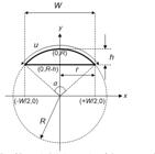
According to the Pythagorean theorem with W=[2R.h-h2] ½, the length of the undulation (e.g., the arc length), of the lens is u=2πR.(α/360). The angle α [º] that defines the area of the circular sector is:
The area of the lens is the area of the circular sector minus the area of the triangle going from the coordinates origin to the interface W of the circular segment and is given by:
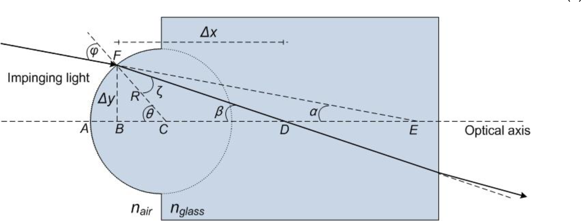
Figure 3 illustrates the refraction caused by a spherical surface and will help in the determination of the refracting power. The amount of a ray that refracts into the point F depends with the radius R. The paraxial approximation is applied to make easy the calculations and because it is a good estimation [14,16]. Thus, in the paraxial approximation the values sin(δ) and tan(δ) are both assumed to be approximately equal to δ. In this case, the Snell’s law becomes equal to:
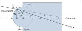
Taking into account that (Equation 6) and substituting the angles φ=θ-α and ζ=θ-β in Equation (5), the relation between R, AD, AE, nair and nglass is obtained and given by Equation 7.
This allows the measurement of how much light refracts towards the optical axis. The numerical indicator of this refraction is the refracting power P given in the equation (7).
The optical power PT in a spherical biconvex lens is the sum of the powers P1=(nglass nair)/R1 and P2=(nair nglass)/R2. According to P. Rathnayaka and coauthors [10] the focal length is defined as the distance from the center of the lens to the image plane where light converges to a similar point named the focal point. The focal length depends on the optical power PT and is given by PT=1/f. Therefore, the focal length of a plano-convex lens is f=R/(nglass 1) because R2=∞.
MICROLENSES: OVERVIEW
A wide range of processes and technologies to fabricate microlenses can be found in the literature, however, the main objective of this review is to present very different techniques and not to present all the variances found in the microlenses fabrication technologies and materials.
The steps to fabricate microlenses in PDMS (polydimethylsiloxane) are depicted in the first image of the provided reference [17]. This fabrication process is straightforward and can be easily adjusted to meet specific requirements, such as altering the size and focal length (f) of the microlenses. In the second image from the same reference [17], an array of microlenses is displayed, along with close-up details of a single microlens, which were obtained using Scanning Electron Microscopy (SEM). It is mentioned that the specifications of the microlenses can be modified by adjusting the liquid (PDMS) injection conditions within the frame [17]. The PDMS is injected on a microfluidic network used to control its flow-rate, thus, controlling the size of the microlenses. The injection pressure is changed and the cavity is being filled with PDMS. Meanwhile, the cavity membrane deforms while is filled with PDMS. Then, the PDMS is cured, resulting in the desired profile, shape and size. This structure presents focal lengths ranging from 1.6mm to tens of millimeters.
The fabrication process of an array of microlenses for collimating purposes is described in reference [18]. In this technique, the microlenses are formed within the bonded layer of a Silicon-On-Insulator wafer. The process involves melting rectangular pads of thick photoresist, which creates a surface tension causing them to rotate out to a new plane. In addition, the same photoresist used in this process also serves to produce the actual lenses by melting circular pads.
To ensure proper alignment of the mount normal to the substrate, a sequential self-assembly of a supporting silicon frame is employed. The resulting array consists of six bi-convex spherical lenses with a focal length of 30µm and a pitch of 80µm. These lenses are formed from circular pads of thick photoresist, each with a diameter of 60µm.
An alternative method for fabricating microlenses was demonstrated by J. Kim and coauthors [19]. In this approach, they utilize direct ink-jet printing of a UV-curable hybrid polymer to create a microlens array. The process involves printing a pattern of polymer drops onto a glass substrate and subsequently curing them under UV light. Through this technique, they are able to produce periodic arrays of approximately semi-spherical microlenses. The microlenses have a diameter of 50μm and a focal distance of 48μm. The benefits of this method, as shown in the reference [19], include large numerical apertures and short focal distances, making it suitable for applications requiring optical interconnects.
An alternative technique for the fabrication of microlens arrays involves the utilization of a mold [20]. This process employs sol-gel glass as the material for creating the lenses, with the aid of an SU-8 mold (master) used to fabricate the replica in PDMS. The fabrication steps and SEM images of the material before and after the softening process are shown in the reference [20]. The PDMS substrate replica, formed using the SU-8 mold on a silicon wafer, serves as the initial mold required for the subsequent fabrication steps.
The replica is then filled with photoresist and the consequent structure obtained is thermally softened turning the upper part of the cylindrical photoresist into a spherical shape. A new PDMS substrate is then used to build a second and final mold, where the sol-gel glass gets the lenses shape (measuring 100µm ×100µm) after a curing treatment.
A very short f was achieved in plano-concave microlens on a two-dimensional photonic crystal made of indium phosphide (InP) and indium gallium arsenide phosphide (InGaAsP) semiconductor with a refraction index smaller than the unity [21].
The photonic crystal's square lattice of air holes and the cross-section of the corresponding structure are shown in the reference [8]. Additionally, a photograph of a single element of a select sample and its corresponding exotic structure is included in the same reference [8]. The microlens featured in this study has a focal length of approximately 12μm at 1500nm. The photonic crystal operates as an isotropic dielectric medium, following Snell's law for refraction. The fabrication process involved etching air holes into the InP/InGaAsP structure, which consists of a top 200nm InP cladding layer, a middle 400nm InGaAsP layer, and a bottom 300μm InP cladding substrate. The microlens exhibits a negative index of refraction, which introduces new and promising possibilities for the development of future optoelectronic devices. Despite the lens having a radius of 20μm, its focal point remains at 12μm due to its negative index nature [8].
Finally, J. Ribeiro and coauthors [22] presents a simple but accurate technique to fabricate microlenses with low-cost and high reproducibility. This technique is so-called hanging droplet method and offers a superior control of the final shape, simply by controlling the processing time. In this process, a micro-pipette controls the volume of PDMS in order to allow the fabrication of microlenses with different thicknesses. First, the droplet is deposited on top of the intended target (which can be a substrate of microsystem or a light source such as a LED).
Then, the PDMS is cured by placing the sample upside down and without heating for 24 hours. Contrary to other techniques, the PDMS surface never touches other materials, ensuring a low-roughness in the surface of PDMS. Moreover, this method combines the simplicity with the elegance to obtain the desired shape only by using the force of gravity.
The microlenses under consideration were incorporated into an optical biopsy microsystem. This microsystem encompasses an image magnification optical module along with light-emitting diodes (LEDs). The microsystem was evaluated by capturing an image of parallel lines with a width of 20μm and spacing of 20μm. The image displayed the characteristic impact of spherical aberration, resulting in significant distortion at the left and right edges. The authors observed that the image magnification optical module accomplished a magnification factor of 4 and achieved a remarkable 30% enhancement in image quality by employing optical irradiance from LED illumination.
The fabrication techniques and processes suffered several changes and improvements across the last twenty years. The same can be observed relatively to the materials selected to fabricate microlenses. The two main materials used are glass and polymer-based materials.
The fabrication processes currently available for polymers include the microjet technique, photoresist reflow, ultraviolet curing, hydrophobic effect, LIGA (Lithographie, Galvanoformung, Abformung) and the soft replica molding methods [23]. The continuous improvements in the material properties of polymers and enhancements on processes and technologies justify the focus on these materials when fabricating microlenses. Table 2 summarizes the several techniques applied on the fabrication of microlenses [24,25].
MICROLENSES: STATE-OF-THE-ART
In this subsection, the main contributions to scientific and technological advancements in the subject in recent years are presented. To achieve this, two systematic review tools, ProKnow-C and Methodi Ordination, were utilized to develop and extract the state-of-the-art information on microlenses [26, 27].
State-of-the-art: Microlenses - ProKnow-C
ProKnow-C is a tool used for systematic literature review and research synthesis [26]. In this case, a ProKnow-C analysis was conducted based on a search query for microlenses and microlens arrays, and the papers were searched in IEEE Xplore, ScienceDirect, and Scopus databases published between 2019 and 2023.
ProKnow-C is systematic literature review tool that can be used for research synthesis, the following structure was used to obtain the results: (1) Identification of search terms and filters: The keywords "optical microsystem," "microlenses," "micro-fabrication," and "CMOS" were used to conduct a search of papers published between 2019 and 2023. (2) Selection of relevant papers: The results were filtered to include only papers related to the review of technologies and applications of microlenses and microlens arrays. After screening, a total of 163 papers were found to be relevant. (3) Extraction of data: The data from the selected papers were extracted and organized into a spreadsheet, which included information such as the title, author, year of publication, journal, and DOI. (4) Calculation of ProKnow-C score: The ProKnow-C score for each paper was calculated based on its citation count, relevance, and impact factor. Table 3 presents the results of the ProKnow-C analysis, listing the 10 most important papers published between 2019 and 2023.
Based on the results of the ProKnow-C, the state-of-the-art in the field of microlenses and microlens arrays that the current state-of-the-art research on microlenses and microlens arrays highlights recent advances in microfabrication techniques that have enabled the production of high-quality and customizable microlenses for use in imaging, sensing, and optical communications applications.
The integration of microlenses with complementary metal-oxide-semiconductor (CMOS) technology has further enabled the development of efficient and compact optical systems. The most significant contributions to the field, identified by the ProKnow-C analysis, provides an overview of microlenses, their properties, and fabrication techniques, as well as their applications in various fields,demonstrates the use of microlenses in optical communication systems, showing significant improvements in data transmission rates and energy efficiency.
State-of-the-art: Microlenses - Methodi Ordinatio
In this study, the researcher utilized Methodi Ordinatio analysis to identify important papers on the topic of microlenses and microlens arrays [27]. The methodology comprises several stages, beginning with the definition of the research question and identification of relevant keywords, such as "microlens," "microlens array," "fabrication," "characterization," and "applications." Subsequently, the researcher performs a systematic search of the literature across various databases to ensure comprehensive coverage of the relevant literature. After identifying the pertinent papers, the researcher extracts essential information, including research question, methodology, results, and conclusions, for subsequent grouping of papers with similar categories focused on microlenses and microlens arrays, as well as the specific techniques utilized for their fabrication and characterization. The results of the Methodi Ordinatio analysis (Table 4), listing the 10 most influential papers (2019-2023) that cover various aspects of microlens fabrication, characterization, and applications.
These papers provide an in-depth review of the latest advancements in microfabrication techniques and materials for microlens fabrication, covering topics such as microlens design, simulation, and fabrication using different techniques.
The significance of these papers lies in their detailed insights into the microlens fabrication process, which has enabled the development of new and improved fabrication techniques, as well as the potential applications of microlenses in optoelectronics, biomedicine, and telecommunications.
The findings of these papers have led to the creation of microlenses with enhanced performance and functionality, thus paving the way for new and exciting applications. Overall, the contributions of these papers have solidified the importance of microlenses as a vital component in many optical systems, with continued advancements expected to have a far-reaching impact in various fields.
State-of-the-art: Comparative analysis ProKnow-C and Methodi Ordinatio
A comparative analysis of the results obtained from the Methodi Ordinatio and ProKnow-C techniques, a consolidated list of the most significant papers was generated. Out of the papers identified by both techniques, five were deemed to be the most important review papers.
The selected papers represent the most impactful research works published between 2019 and 2023 on the topic of microlenses fabrication technologies, characteristics, and applications.
The criteria for the selection of these papers were based on their relevance, scientific rigor, and contribution to the field. These papers were deemed significant due to their novel approaches and contributions to the field of optical microsystems and microlens arrays. The results of the comparative analysis showed the Table 5, listing the 9 most important review papers published between 2019 and 2023.
The present study conducted Methodi Ordinatio and ProKnow-C analyses to identify the most important review papers on the fabrication methods, characteristics, and applications of microlenses and microlens arrays. After comparing the results of the two analyses, the study identified the following five papers as the most important resources for researchers in this field:
The ranking of these papers as the most important is based on their comprehensive coverage of the different fabrication methods, characteristics, and applications of microlenses and microlens arrays, emphasizing their feasibility for various uses and illustrating the trend towards emerging techniques and optimization of performance. In conclusion, the unified list of significant papers, which is based on results obtained from Methodi Ordinatio and ProKnow-C analyses, establishes the current state-of-the-art in the field of microlenses and microlens arrays.
MICROLENSES: A CASE STUDY
A fabrication process of microlenses was developed for application on silicon-based microsystems [56, 57]. The intention was to fabricate the microlenses directly on top of the microsystem. The microsystem was mainly composed by photodetectors to make optical transduction, by the electronics for readout, conversion and interface, and of course, by the microlenses itself. Both the photodetectors and the electronics are fabricated in CMOS technology to achieve the most as possible compactness and miniaturization. The fabrication process has to be compatible with CMOS technology for enjoying all of its imaging advantages while overcoming high optical and electronic crosstalks. Therefore, a process for fabricating arrays of microlenses with high-aspect ratio for enhancing light acquisition (which otherwise would be scattered away) was developed. The microlenses were fabricated directely on top of a substrate capable to transduce more efficiently photons into photocurrent.
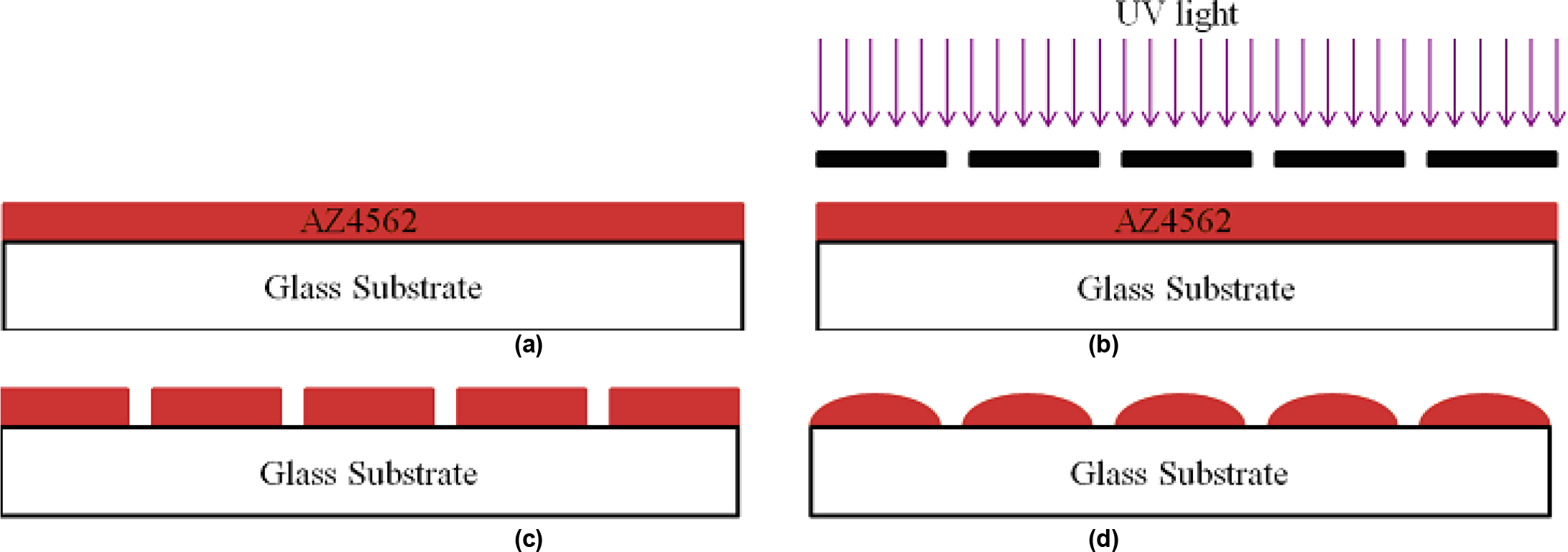
Standard processes found on microfabrication, more precisely, photolithography and thermal reflow of photoresists were applied in the fabrication of refractive microlenses with spherical shape (viewed on cross-section) [25,26]. These methods and technologies allow the reproducible fabrication of microlenses with three dimensional microstructures. Additionally, this technique allowed the customization of optical microcomponents with high-quality and cost effectiveness. Figure 4 illustrates the fabrication steps used in the fabrication of the microlenses, where in the first step (a c), arrays of strips with rectangular shapes are patterned using a conventional lithography process. In the second step (d), the strips are subjected to a reflow process. This second step consists on heating the strips until becoming viscous and thus, giving origin to surface tensions, reflowing the material and forming a surface with the desired lenticular shape.
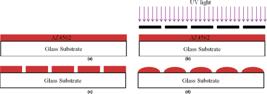
Steps involved in the fabrication of microlenses: (a) spin coating and prebake of the photoresist, (b) UV exposure of the photoresist, (c) development of the photoresist, and (d) the thermal reflow of the photoresist to obtain the actual lens profile [56].
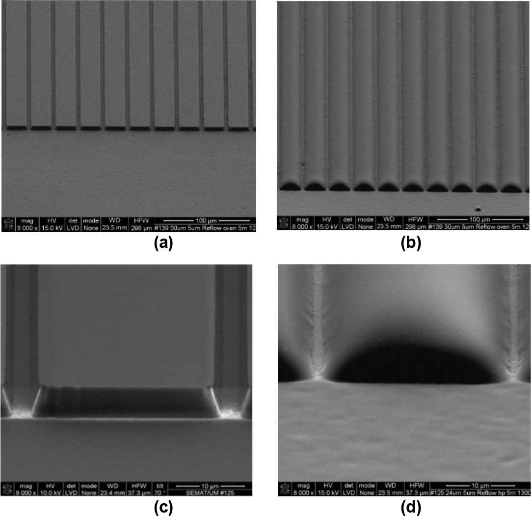
This technique allows the fabrication of high quality spherical and parabolic shaped microlenses by heating up the photoresist above its glass transition temperature. The array with the desired shape was designed and printed into a chromium mask. Then, the AZ4562 photoresist was selected due to the fabrication requirements. This positive photoresist is ideal to coat substrates with thicknesses above 3μm to 5μm without the need to increase the exposure energy considerably and still, providing enough energy down to the substrate of the AZ4562 material. Figure 5 shows few functional prototypes (a) before and (b) after the thermal reflow of the photoresist. Figure 5 also shows SEM images of a single lens of an array selected sample (c) before and (d) after the thermal reflow and rehydration. The most important fabrication process steps and parameters are listed in Table 6. These fabrication settings were selected to obtain microlenses with 26µm measured within their interface with the substrate and with apexes 5µm thick (sag height).
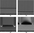
SEM images of few functional prototypes (a) before and (b) after the thermal reflow of the photoresist. SEM images of a single lens of an array selected sample (c) before and (d) after the thermal reflow and rehydration.
Several tests were made with a CMOS photodiode with a square shape and 24µm in size, without microlenses to determine the photocurrent response under white and red lights.
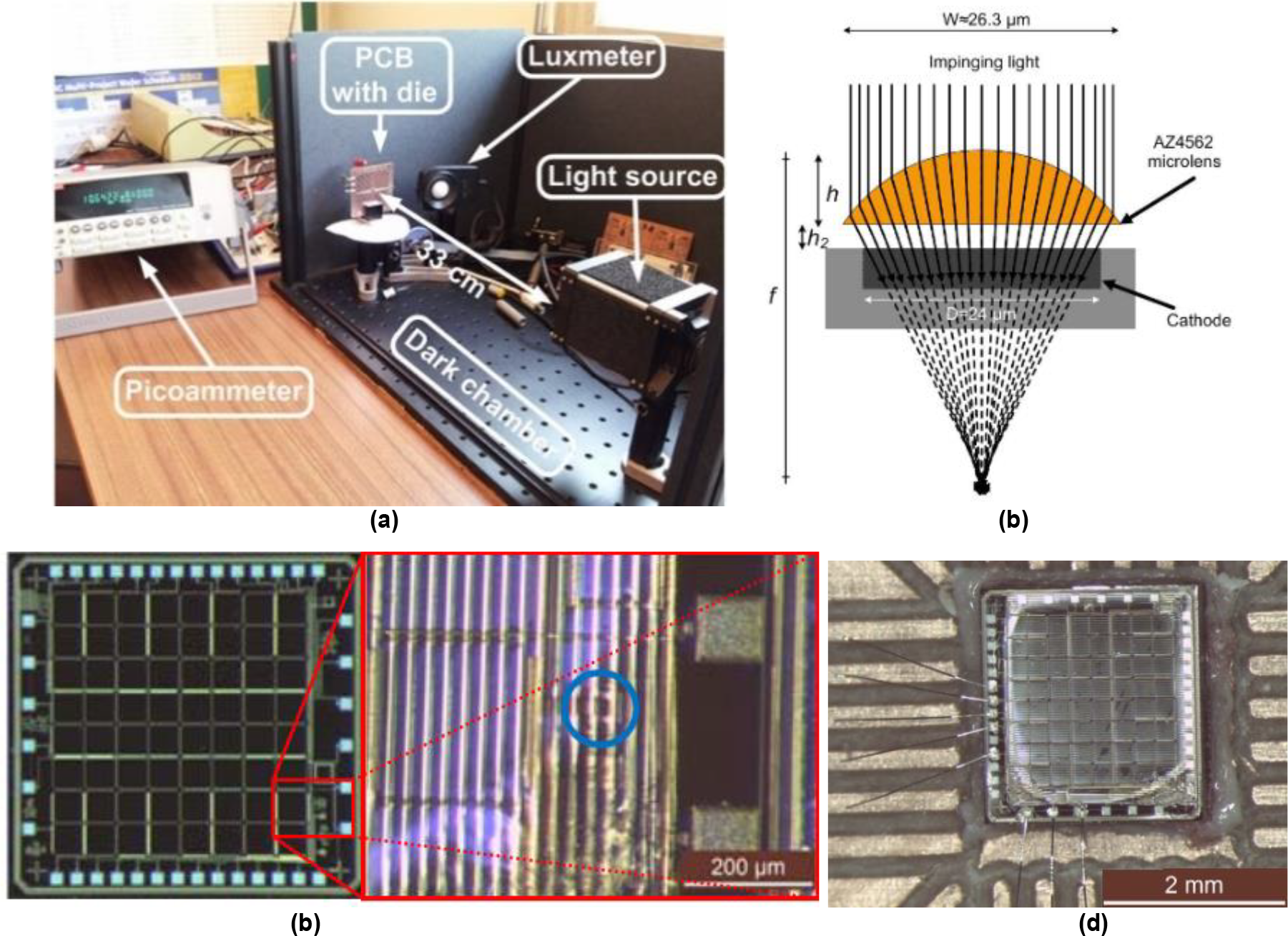
The work presented in [56] only studies the effect of red light with and without the microlenses. The work done by J. M. Gomes and coauthors [58] presents the fully study of the effect of the white light with and without the microlenses and at the same time, compares the results with red light. Two bias voltages of 0V and 4V were used as parameters. Figure 6(a) shows the custom made test setup, which comprises a dark chamber, two light sources, collimation lens for obtaining a parallel light beam, a luxmeter model CET CT 1330B High Accuracy Lux Digital Light Meter with a resolution of 0.1 lux for measuring and calibrating the impinging light’s optical power and a picoammeter model Keithley 6487 Picoammeter Voltage Source with a resolution of 10-14A [56]. The light source is digitally controlled by a programmable development board, subjecting the photodiodes to a linear increment of the illuminance from 0 to 2000 lux. Figure 6(b) and (c) shows the measuring concept and an optical microscopy photograph of the 24µm squared photodiode (surrounded by a blue circle) below an array of microlenses that was already fabricated on top of the CMOS microdevice that contains the photodiode [56]. This microdevice was designed and fabricated in the 0.7µm CMOS technology from the on-semiconductor (formerly AMIS, Alcatel MIETEC).
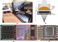
(a) Photograph of the setup that was used for characterizing the photodiode without and with microlenses. (b) The measuring concept and (c) an optical microscope photograph of the fabricated microdevice (the full CMOS microdevice is showed on left for illustration purposest) with the microlens fabricated on top of the photodiode. The apex of the microlens is aligned with the center of the 24µm square photodiode (blue circle). (d) A photograph of a zoom showing a CMOS
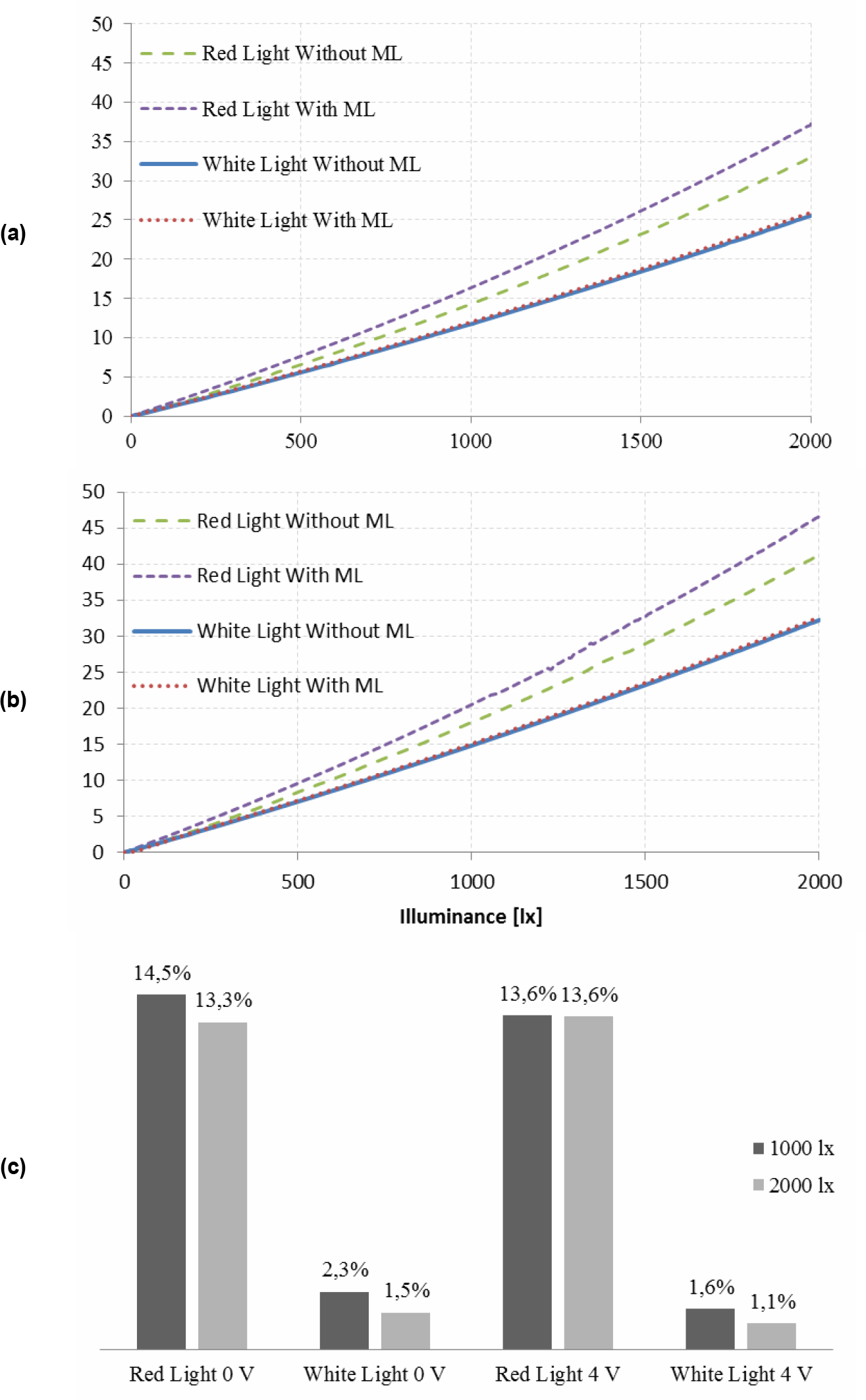
By fabricating microlenses with a width larger than the photodiode active area directly on the silicon substrate it is possible to enhance the production of photocurrent on CMOS photodiodes. This is possible by redirecting light into the active area that otherwise would fall outside. A photomask with rectangular strips was used to fabricate microlenses on top of a 24µm photodiode. Figure 7 shows the results before and after the fabrication of microlenses. These results were obtained with red and white light sources and increasing the illuminance from 0 lux up to 2000 lux. Additionally, a reverse bias voltage of either 0V or 4V was applied into the photodetector.
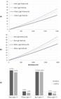
Comparison between the photocurrents measured for different reverse bias voltages of (a) 0V and (b) 4V under red and white light, without and with the 26µm microlens on a 24µm squared photodiode. (c) The efficiency improvement [%] achieved at different illuminance values.
It was observed an improvement in the photocurrent with microlenses above the photodiode, e.g., an improvement of ≈14% and ≈2% with red and white lights, respectively. The difference between the two results is due to the different spectral transmittances of the photoresist observed for both light compositions [25].
Other microlenses with other dimensions were also fabricated by R. P. Rocha [47] using this same technique. The full characterization and the measurement of the focal length of these new microlenses was performed using the experimental setup fully described in the same reference [47]. These measurements demonstrated the feasibility to fabricate large series of microlenses with a width of 35µm, spaced apart by 3µm and 5µm thick. The focal length was 49µm with a measured tolerance of ±2µm, e.g., corresponding to a maximum error of ±4%. These results leaded to a numerical aperture of 33.6×10 2 with a tolerance of ±1.3×10 2. The measurements also showed an f number of 1.4.
To finish, it must be noted that a complete study was conducted by Gomes, J.M. and coauthors on arrays of microlenses fabricated with this method and using the same fabrication parameters on Table 6. This study consisted on a statistical analysis applied into the shape of the microlenses. Theirs results successfully validated the requirement for reproducibility, making this fabrication process feasible on high-volume production of arrays of microlenses [58].
CONCLUSIONS
This paper presented a review of microlenses for Microsystems, e.g., it have described fabrication technologies, characteristics and applications of microlenses. A case study was also presented in this paper, where polymeric microlenses were fabricated using standard techniques found in the microelectronics industry (e.g., photolithography) and an additional post-processing step (e.g., the thermal reflow and rehydration). The optical characteristics of these microlenses were also obtained (e.g., the focal distance, the numerical aperture and the f-number). Finally, the feasibility to augment light into photodiodes was also demonstrated fabricating a microlens on top of a CMOS photodetector that was fabricated in the 0.7µm CMOS technology from the on-semiconductor (formerly AMIS, Alcatel MIETEC).
-
Funding:
This work was partially supported by the Brazilian agency National Council of Scientific Research (Conselho Nacional de Desenvolvimento Científico e Tecnológico, CNPq) under the grant 400110/2014-8: MEC/MCTI/CAPES/CNPQ/FAPS. Rodrigo Henrique Gounella was supported with a MSc scholarship granted by the Brazilian agency CAPES. Professor João Paulo Carmo was also supported by the Pesquisador de Pró-actividade (PQ) scholarship from the CNPq under the grant 305250/2015-9. The authors also acknowledge to Dr. Ing Christian Koch from the company MicroChemicals GmbH for the technical support. This work was partially supported by FCT national funds, under the national support to R&D units grant, through the reference project UIDB/04436/2020 and UIDP/04436/2020. This research was also partially supported by the FAPESP agency (Fundação de Amparo à Pesquisa do Estado de São Paulo) through the project with the reference 2019/05248-7. J.P.C. was support by a PQ scholarship with the reference CNPq 304312/2020-7.
Acknowledgments:
The authors would like to thank the support of the Coordination for the Improvement of Higher Education Personnel - CAPES, Foundation for the Support of Science and Technology of Pernambuco - FACEPE, the Brazilian National Council for Scientific and Technological Development - CNPq.
Data Availability Statement:
Research data are only available upon request for corresponding author.
REFERENCES
- 1 Molesini G. Early advances on rays and refraction: a review through selected illustrations. Opt. Eng. 2011;50(12):121704.
- 2 Matoba O, Tajahuerce E, Javidi B. Three-dimensional object recognition based on multiple perspectives imaging with microlens arrays. In: Proceedings of the 14th Annual Meeting of the IEEE Lasers and Electro-Optics Society (LEOS 2001); 2001.
- 3 Carlson K, Chidley M, Sung K, Descour M, Gillenwater A, Follen M, Richards-Kortum R. In vivo fiber-optic confocal reflectance microscope with an injection-molded plastic miniature objective lens. Appl. Opt. 2005;44:1792-7.
- 4 Nikolas C, Gang L, Ki-Hun J, Luke L. Tunable liquid-filled microlens array integrated with microfluidic network. Opt. Express. 2003;11:2370-8.
- 5 Hamam H. A two-way optical interconnection network using a single mode fiber array. Opt. Commun. 1998;150:270-6.
- 6 Van Overmeire S, Volckaerts B, Ottevaere H, Pappaert K, Desmet G, Thienpont H. Simulation, fabrication and characterization of microlens oriented fluorescence detection systems for DNA microarrays. In: Proceedings of the IEEE/LEOS Benelux Chapter Symposium; 2005; Mons.
-
7 Gauri S, Abidin ZZ, Kamuri MF, Mahdi MA, Md Yunus NA. Detection of Aeromonas hydrophila using fiber optic microchannel sensor. J. Sens. 2017:8365189. doi: 10.1155/2017/8365189
» https://doi.org/10.1155/2017/8365189 - 8 Qin S, Shang J, Ma M, Zhang L, Lai C, Huang QA, Wong CP. Fabrication of micro-polymer lenses with spacers using low-cost wafer-level glass-silicon molds. IEEE Trans. Compon. Packag. Manuf. Technol. 2013;3(12):2006-13.
-
9 Zeng L, Li D. Development of in situ sensors for chlorophyll concentration measurement. J. Sens. 2015:903509. doi: 10.1155/2015/903509
» https://doi.org/10.1155/2015/903509 -
10 Rathnayaka P, Baek SH, Park SY. An efficient calibration method for a stereo camera system with heterogeneous lenses using an embedded checkerboard pattern. J. Sens. 2017:6742615. doi: 10.1155/2017/6742615
» https://doi.org/10.1155/2017/6742615 -
11 Zhang L, Tian W, Meng Q, Sun M, Li N, Lei Z. Analysis on structural stress of 64 × 64 InSb IRFPAs with temperature dependent elastic underfill. J. Sens. 2014:952323. doi: 10.1155/2014/952323
» https://doi.org/10.1155/2014/952323 - 12 Born M, Wolf E. Principles of optics: electromagnetic theory of propagation, interference and diffraction of light. 7th ed. Cambridge: Cambridge University Press; 2002.
-
13 Morisawa M, Muto S. Plastic optical fiber sensing of alcohol concentration in liquors. J. Sens. 2012:709849. doi: 10.1155/2012/709849
» https://doi.org/10.1155/2012/709849 - 14 Hecht E. Optics. 4th ed. Boston: Addison-Wesley; 2002.
- 15 Popovic Z, Sprague R, Connell G. Technique for monolithic fabrication of microlens arrays. Appl. Opt. 1998;27(7):1281-4.
- 16 Kenyon IR. The light fantastic: a modern introduction to classical and quantum optics. 2nd ed. Oxford: Oxford University Press; 2011.
- 17 Hongbin Y, Guangya Z, Siong C, Feiwen L. Simple method for fabricating solid microlenses with different focal lengths. IEEE Photonics Technol. Lett. 2008;20(19):1624-6.
- 18 Syms R. Refractive collimating microlens arrays by surface tension self-assembly. IEEE Photonics Technol. Lett. 2000;12(11):1507-9.
- 19 Kim J, Brauer N, Fakhfouri V, Boiko D, Charbon E, Grutzner G, et al. Hybrid polymer microlens arrays with high numerical apertures fabricated using simple ink-jet printing technique. Opt. Mater. Express. 2011;1(2):259-69.
- 20 Orhan J, Parashar V, Sayah A, Gijs M. Fabrication and characterization of three-dimensional microlens arrays in sol-gel glass. J. Microelectromech. Syst. 2006;15(5):1159-64.
- 21 Casse B, Lu W, Huang Y, Sridhar S. Nano-optical microlens with ultrashort focal length using negative refraction. Appl. Phys. Lett. 2008;93(5):053111.
- 22 Ribeiro JF, Costa AC, Gomes JM, Costa CG, Gonçalves SB, Wolffenbuttel RF, Correia JH. PDMS microlenses for optical biopsy microsystems. IEEE Trans. Ind. Electron. 2017;64(12):9683-90.
- 23 Rocha RP, Maciel MJ, Gomes JM, Carmo JP, Correia JH. Fabricating microlenses on photodiodes to increase the light-current conversion efficiency. IEEE Sens. J. 2014;14(5):1343-4.
- 24 Ho J, Shih T, Cheng J, Sung C, Chen C. A novel method for fabrication of self-aligned double microlens arrays. Sens. Actuators A Phys. 2007;135(2):465-71.
- 25 Ottevaere H, Cox R, Herzig H, Miyashita T, Naessens K, Taghizadeh M, et al. Comparing glass and plastic refractive microlenses fabricated with different technologies. J. Opt. A Pure Appl. Opt. 2006;8(7):407-29.
-
26 Maciel JN, Giménez Ledesma JJ, Ando Junior OH. Forecasting solar power output generation: a systematic review with the Proknow-C. IEEE Lat. Am. Trans. 2021 Apr;19(4):612-24. doi: 10.1109/TLA.2021.9448544
» https://doi.org/10.1109/TLA.2021.9448544 -
27 Regatieri HR, Ando Junior OH, Salgado JRC. Systematic review of lithium-ion battery recycling literature using ProKnow-C and Methodi Ordinatio. Energies. 2022;15:1485. doi: 10.3390/en15041485
» https://doi.org/10.3390/en15041485 -
28 Pan M, Fu Y, Zheng M, Chen H, Zang Y, Duan H, et al. Dielectric metalens for miniaturized imaging systems: progress and challenges. Light Sci. Appl. 2022;11(1):195. doi: 10.1038/s41377-022-00885-7
» https://doi.org/10.1038/s41377-022-00885-7 -
29 Gonzalez-Hernandez D, Varapnickas S, Bertoncini A, Liberale C, Malinauskas M. Micro-optics 3D printed via multi-photon laser lithography. Adv. Opt. Mater. 2023;11(10):2201701. doi: 10.1002/adom.202201701
» https://doi.org/10.1002/adom.202201701 -
30 Wu J, Guo Y, Deng C, Zhang X, Li D, Li D, et al. An integrated imaging sensor for aberration-corrected 3D photography. Nature. 2022;612(7938):62-71. doi: 10.1038/s41586-022-05306-8
» https://doi.org/10.1038/s41586-022-05306-8 -
31 Kim M, Kim M, Lee G, Sunwoo S, Chang S, Song Y, et al. Bio-inspired artificial vision and neuromorphic image processing devices. Adv. Mater. Technol. 2021;6(12):2100144. doi: 10.1002/admt.202100144
» https://doi.org/10.1002/admt.202100144 -
32 Dai B, Zhang L, Zhao C, Chen Y, Huang W, Liu Y, et al. Biomimetic apposition compound eye fabricated using microfluidic-assisted 3D printing. Nat. Commun. 2021;12:6458. doi: 10.1038/s41467-021-26606-z
» https://doi.org/10.1038/s41467-021-26606-z -
33 Li KH, Fu WY, Choi HW. Chip-scale GaN integration. Prog. Quantum Electron. 2020;70:100247. doi: 10.1016/j.pquantelec.2020.100247
» https://doi.org/10.1016/j.pquantelec.2020.100247 -
34 Magazine R, van Bochove B, Borandeh S, Seppälä J. 3D inkjet-printing of photo-crosslinkable resins for microlens fabrication. Addit. Manuf. 2022;50:102534. doi: 10.1016/j.addma.2021.102534
» https://doi.org/10.1016/j.addma.2021.102534 -
35 Cao H, Čižmár T, Turtaev S, Tyc T, Rotter S. Controlling light propagation in multimode fibers for imaging, spectroscopy, and beyond. Adv. Opt. Photonics. 2023;15:524-612. doi: 10.1364/AOP.484471
» https://doi.org/10.1364/AOP.484471 -
36 Sala F, Castriotta M, Paiè P, Farina A, D’Annunzio S, Zippo A, et al. High-throughput 3D imaging of single cells with light-sheet fluorescence microscopy on chip. Biomed. Opt. Express. 2020;11:4397-4407. doi: 10.1364/BOE.401386
» https://doi.org/10.1364/BOE.401386 -
37 Debaes C, Thienpont H, Van Daele P, Van Campenhout J, Van Steenberge G, Demeester P, et al. Low-cost microoptical modules for MCM level optical interconnections. IEEE J. Sel. Top. Quantum Electron. 2003 Mar-Apr;9(2):518-30. doi: 10.1109/JSTQE.2003.813316
» https://doi.org/10.1109/JSTQE.2003.813316 -
38 Yuan C, Kowsari K, Panjwani S, Chen Z, Wang D, Zhang B, et al. Ultrafast three-dimensional printing of optically smooth microlens arrays by oscillation-assisted digital light processing. ACS Appl. Mater. Interfaces. 2019 Oct 30;11(43):40662-8. doi: 10.1021/acsami.9b14692
» https://doi.org/10.1021/acsami.9b14692 -
39 Liu X, Yu L, Yang S, Chen Q, Wang L, Juodkazis S, et al. Optical nanofabrication of concave microlens arrays. Laser Photonics Rev. 2019;13(6):1800272. doi: 10.1002/lpor.201800272
» https://doi.org/10.1002/lpor.201800272 -
40 Bae SI, Kim K, Yang S, Jang K, Jeong KH. Multifocal microlens arrays using multilayer photolithography. Opt. Express. 2020;28(6):9082-8. doi: 10.1364/OE.385579
» https://doi.org/10.1364/OE.385579 -
41 Elsherif M, Hassan MU, Yetisen AK, Butt H. Hydrogel optical fibers for continuous glucose monitoring. Biosens. Bioelectron. 2019;137:25-32. doi: 10.1016/j.bios.2019.05.002
» https://doi.org/10.1016/j.bios.2019.05.002 -
42 Ratcliff J, Supikov A, Alfaro S, Azuma R. ThinVR: Heterogeneous microlens arrays for compact, 180 degree FOV VR near-eye displays. IEEE Trans. Vis. Comput. Graph. 2020 May;26(5):1981-90. doi: 10.1109/TVCG.2020.2973064
» https://doi.org/10.1109/TVCG.2020.2973064 -
43 Wang W, Chen G, Weng Y, Yu J, Xiong Y, Zhou H, et al. Large-scale microlens arrays on flexible substrate with improved numerical aperture for curved integral imaging 3D display. Sci. Rep. 2020;10:11741. doi: 10.1038/s41598-020-68620-z
» https://doi.org/10.1038/s41598-020-68620-z -
44 Zhang Q, Schambach M, Schlisske S, Jin Q, Mertens A, Rainer C, et al. Fabrication of microlens arrays with high quality and high fill factor by inkjet printing. Adv. Opt. Mater. 2022;10(19):2200677. doi: 10.1002/adom.202200677
» https://doi.org/10.1002/adom.202200677 -
45 Zhang T, Li P, Yu H, Wang F, Wang X, Yang T, et al. Fabrication of flexible microlens arrays for parallel super-resolution imaging. Appl. Surf. Sci. 2020;504:144375. doi: 10.1016/j.apsusc.2019.144375
» https://doi.org/10.1016/j.apsusc.2019.144375 -
46 Zhang L, Naples N, Zhou W, Yi AY. Fabrication of infrared hexagonal microlens array by novel diamond turning method and precision glass molding. J. Micromech. Microeng. 2019;29(6):065004. doi: 10.1088/1361-6439/ab10ff
» https://doi.org/10.1088/1361-6439/ab10ff -
47 Liu Z, Wang D, Gao H, Li M, Zhou H, Zhang C. Metasurface-enabled augmented reality display: A review. Adv. Photonics. 2023 May;5(3):034001. doi: 10.1117/1.AP.5.3.034001
» https://doi.org/10.1117/1.AP.5.3.034001 -
48 Cheng Y, Cao J, Zhang Y, Hao Q. Review of state-of-the-art artificial compound eye imaging systems. Bioinspir. Biomim. 2019;14(3):031002. doi: 10.1088/1748-3190/aaffb5
» https://doi.org/10.1088/1748-3190/aaffb5 -
49 Park J, Brady DJ, Zheng G, Tian L, Gao L. Review of bio-optical imaging systems with a high space-bandwidth product. Adv. Photonics. 2021 Jul;3(4):044001. doi: 10.1117/1.AP.3.4.044001
» https://doi.org/10.1117/1.AP.3.4.044001 -
50 Li Y, Hong M. Parallel laser micro/nano-processing for functional device fabrication. Laser Photonics Rev. 2020;14:1900062. doi: 10.1002/lpor.201900062
» https://doi.org/10.1002/lpor.201900062 -
51 Gao S, Yang K, Shi H, Wang K, Bai J. Review on panoramic imaging and its applications in scene understanding. IEEE Trans. Instrum. Meas. 2022;71:5026034. doi: 10.1109/TIM.2022.3216675
» https://doi.org/10.1109/TIM.2022.3216675 -
52 Hepp S, Jetter M, Portalupi SL, Michler P. Semiconductor quantum dots for integrated quantum photonics. Adv. Quantum Technol. 2019 Sep;2(9):1900020. doi: 10.1002/qute.201900020
» https://doi.org/10.1002/qute.201900020 -
53 Zuo C, Chen Q. Computational optical imaging: Where it comes from, where it is, where it goes, and where it should go. Hongwai Yu Jiguang Gongcheng (Infrared Laser Eng.) 2022 Feb 25;51(2):20220110. doi: 10.3788/IRLA20220110
» https://doi.org/10.3788/IRLA20220110 -
54 Măriuţa D, Colin S, Barrot-Lattes C, Le Calvé S, Korvink JG, Baldas L, et al. Miniaturization of fluorescence sensing in optofluidic devices. Microfluid. Nanofluidics. 2020 Sep;24(9):65. doi: 10.1007/s10404-020-02371-1
» https://doi.org/10.1007/s10404-020-02371-1 -
55 Phan HL, Yi J, Bae J, Ko H, Lee S, Cho D, et al. Artificial compound eye systems and their application: a review. Micromachines. 2021;12:847. doi: 10.3390/mi12070847
» https://doi.org/10.3390/mi12070847 -
56 Rocha RP, Belsley MS, Correia JH, Carmo JP. Low f-number microlenses for integration on optical microsystems. IEEE Sens. J. 2015 Jul;15(7):4073-5. doi: 10.1109/JSEN.2014.2385476
» https://doi.org/10.1109/JSEN.2014.2385476 -
57 Emadi A, Wu H, Grabarnik S, De Graaf G, Hedsten K, Enoksson P, et al. Fabrication and characterization of IC-compatible linear variable optical filters with application in a micro-spectrometer. Sens. Actuators A Phys. 2010;162(2):400-5. doi: 10.1016/j.sna.2010.04.029
» https://doi.org/10.1016/j.sna.2010.04.029 -
58 Gomes JM, Rocha R, Correia JH, Carmo JP. Microlenses and photodetectors integration for augmenting photocurrent. In: 2014 29th Symposium on Microelectronics Technology and Devices (SBMicro). 2014. doi: 10.1109/SBMicro.2014.6940110
» https://doi.org/10.1109/SBMicro.2014.6940110
-
Editor-in-Chief:
Paulo Vitor Farago
-
Associate Editor:
Paulo Vitor Farago